

The automation level of the PCB manufacturing process is high, and it allows for quantitative control of the processing, providing the product with unparalleled consistency. At the same time, through the lamination process, it ensures that the PP (prepreg) is fully squeezed and filled into the copper coils on the PCB, ensuring good insulation.
Detail
The stator poles of an axial flux motor are arranged along the axis, and the rotor is typically a cylindrical structure. The magnetic flux passes through the central axis of the rotor. When current flows through the stator windings, it generates a magnetic field that passes through the rotor in the axial direction. According to the Lorentz force law, this magnetic field produces a torque in the rotor, thereby driving the rotor to rotate.
Detail
Direct Attach Cable (DAC) is a type of twisted-pair network cable used for connecting switches, routers, and servers in networking setups. Depending on the requirements of the connected devices, DAC cables can transmit data at speeds of 10Gbps, 25Gbps, 40Gbps, 50Gbps, and 100Gbps. The length of DAC cables can be customized according to actual needs, with common options including 1m, 3m, 5m, 7m, and 10m.
Detail
Optical devices, which include optical chips and optical component assemblies, account for over 70% of the cost of optical modules. Auxiliary materials, such as housings, pins, PCBs, and circuit chips, make up nearly 30% of the total cost of optical modules.
Detail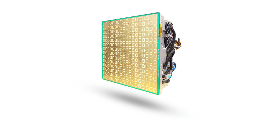
The phased array system generally accounts for nearly 50% of the total cost of the radar system, and the T/R module accounts for about 45% of the phased array system cost, with the RF chip having the largest share.
Detail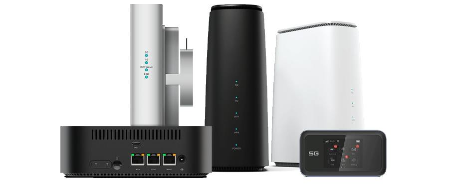
FWA (Fixed Wireless Access) is a technology that combines fixed-line and wireless communication, specifically designed to offer broadband access services to users.
Detail WeChat
