
Backplanes can be used to connect multiple devices, modules, or circuit boards together to achieve high-speed data transmission, signal transmission, and control functions. Backplanes typically have multiple connectors that can be inserted into different modules or circuit boards and connected through high-speed signal lines or optical fibers.
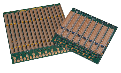
CompactPCI Backplane
Backplanes can provide high bandwidth, low latency, and reliable connectivity, and are widely used in communication equipment, network equipment, servers, computers, and other fields.
Considering that the backplane needs to withstand high-frequency, high-capacity high-speed signal transmission, the backplane PCB design needs to consider electrical performance, mechanical performance, reliability, heat dissipation performance, and other aspects. During manufacturing, high-performance materials and high-precision processing techniques are required to ensure that the backplane PCB meets performance requirements and works stably.
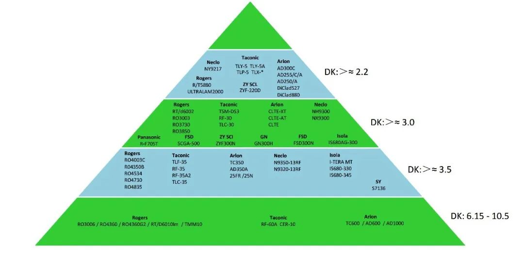
Backplanes typically use FR4-TG170 or higher grade boards, which have higher glass transition temperatures and better flame resistance than ordinary FR4-TG130. Usually, boards with a dielectric constant ε (Dk) of no bigger than 4.4 are selected to reduce signal crosstalk.
High-Speed Materials for PCB
The stacking design of the backplane PCB needs to comply with the following principles:
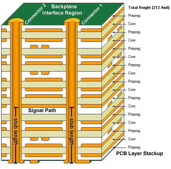
Stacking principle: In a backplane PCB, there are usually signal layers, power planes, and ground planes. The ground plane and power plane can provide a low-impedance current return path for adjacent signal traces. The signal layers should be located between the power or ground reference plane layers, forming symmetrical or asymmetric striplines.
Dividing power domains: There are multiple power supplies on the backplane, such as -48V, 12V, 3.3V, etc. The number of wiring layers for each power supply needs to be determined based on the current requirements of each power supply. At the same time, the power plane needs to be closely coupled with the ground plane to reduce common-mode EMI interference.
Signal layer: When routing signal lines on adjacent layers, follow the vertical routing rule. It is best to avoid crossing reference planes in the path of high-speed signal routing. If it is necessary to cross reference planes, bypass capacitors need to be placed at the gaps between different plane divisions. This ensures continuous impedance of the signal lines and reduces signal reflection and crosstalk.
Ground plane: Set multiple ground planes where possible to provide a low-impedance current return path. Consider using thin PP to increase the coupling between the ground plane and signal layers or ground planes.
Maintain symmetrical stacking: When designing the stacking, try to make the signal layer, power layer, and ground plane layer symmetrical. If there is a situation where the signal layer corresponds to the power layer or ground plane layer, cover the ground copper in the area where there is no signal routing on the signal layer, so as to ensure a symmetrical structure as much as possible and avoid warping during the processing.
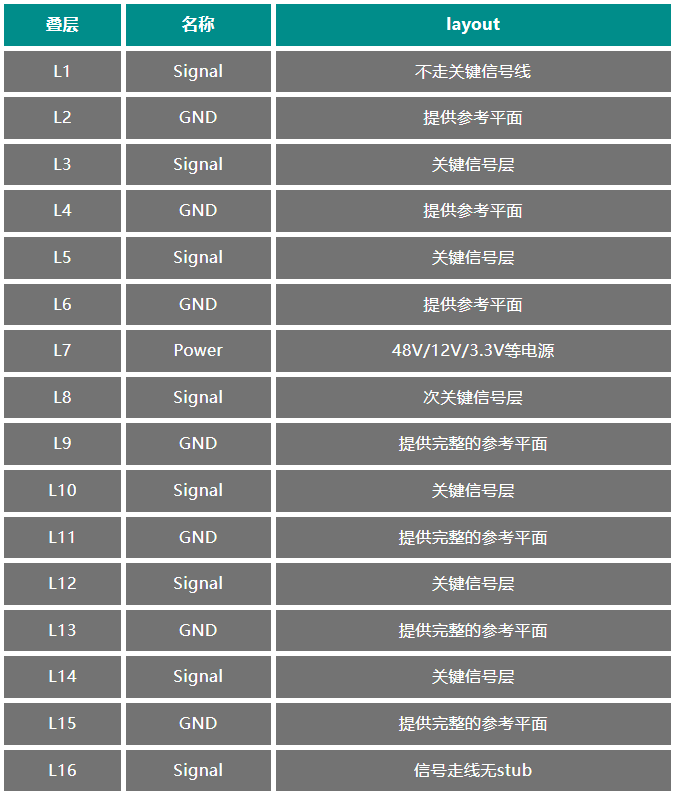
The laminated design of the 16-layer backplane is as follows:
Some backplanes need to consider multiple types of model line routing, as well as the function of powering various boards. For example, the OpenVPX backplane requires a total current of up to 100A carrying multiple voltages.
At this time, multiple power planes are needed to meet the current demand. A segmented strategy can be used to separate the power plane from the high-speed signal line area within the same layer, as shown in the following figure.
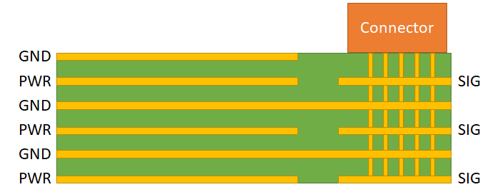
If the number of layers of the PCB allows, use ground planes to separate each power supply layer, ensuring that the signal lines have a good reference plane while also ensuring that the entire PCB has good shielding.
There are 3 types of signals on the backplane: clock bus, management bus, and high-speed signals.
Clock bus signals are all differential signals, such as M-LVDS level multi-point low voltage differential signaling, which allows multiple drivers or receivers to share the same physical link. The clock bus design follows the following principles:
1.Place a 100Ω termination resistor near the source and end of the clock bus to absorb the reflected signal to the maximum extent.
2.The length of the clock bus cannot exceed the driving capability of the chip.
3.The number of vias through which the clock bus passes should not exceed two, reducing the parasitic capacitance caused by vias. Ground vias should be placed nearby to provide the shortest return path for AC signals. The presence of each via can cause discontinuities in signal impedance.
4.The clock bus spacing should follow the 3W principle to minimize crosstalk between signals.
5.The routing of the bus needs to be accompanied by a complete reference plane to ensure the shortest path for the return flow of the bus signal, while ensuring that the characteristic impedance does not undergo sudden changes.
6.The characteristic impedance of the differential line is 100Ω.
The management bus signal is a single-ended signal, and the physical interface form is I2C. The management bus design follows the following principles:
1.The management bus source and end are connected to a pull-up 4.7K resistor to improve the drive capability of the bus and absorb some reflections.
2.The length of the management bus cannot exceed the driving capability of the chip.
3.The characteristic impedance of the single-ended signal line is designed to be 65Ω.
The high-speed signal lines are mainly the data exchange bus between the service board and the switch board and the data bus between the neighboring service boards, all of which are high-speed differential signal lines. The high-speed signal lines follow the following design principles:
1.Try not to use more than two vias for differential lines to reduce parasitic capacitance caused by vias, and create nearby ground vias near the vias to provide the shortest return path for AC signals.
2.The differential line needs to adopt the 3W principle with other network spaces to minimize crosstalk.
3.The routing of differential lines requires a complete reference plane to ensure the shortest return path for bus signals and no sudden changes in characteristic impedance.
4.The differential pairs adopt a strictly equal length routing method to ensure stable signal timing within the differential pairs.
The characteristic impedance of the differential line is designed to be 100Ω.
With the development of electronic packaging, components and systems towards miniaturization and high density, the requirements for data transmission rate are increasingly high, and connectors are gradually developing towards micro-pitch, multi-row pins, and high density. Ordinary soldering connectors have been unable to meet design requirements and are gradually being replaced by crimping connectors. The failure rate of crimping connections is an order of magnitude lower than that of ordinary soldering (no thermal shock, thermal damage).
The crimping process is a connection formed by fitting flexible or rigid pins with metallized holes on a printed circuit board at room temperature. Relying on the interaction between metals, a close contact similar to the molten state of atoms is formed between the pins and the metallized holes, achieving mechanical and electrical connection between the connector and the printed circuit board wires.
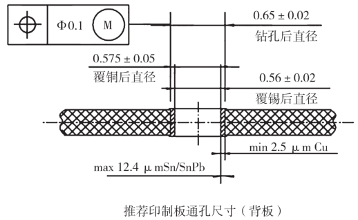
To ensure the yield of connector crimping, the backplane requires strict control of the hole diameter tolerance of the backplane connector. Taking the VPX backplane connector as an example, the following figure shows the tolerances that need to be controlled for PCB drilling.
When we design the backplane and run business tests in the chassis with business boards, we often notice that the speed cannot be increased or there are more serious packet loss problems due to impedance discontinuity caused by connectors between the business boards and the backplane, resulting in signal integrity issues. However, most of the time, the impedance discontinuity actually originates from vias.
Plated through-holes (PTH) can introduce jitter, attenuation, and higher bit error rates for high-speed signals. The higher the signal rate, the greater the signal distortion caused by PTH vias. The distortion of PTH vias at 6.25Gb/s is typically more than twice as large as the distortion at 3.125Gb/s.
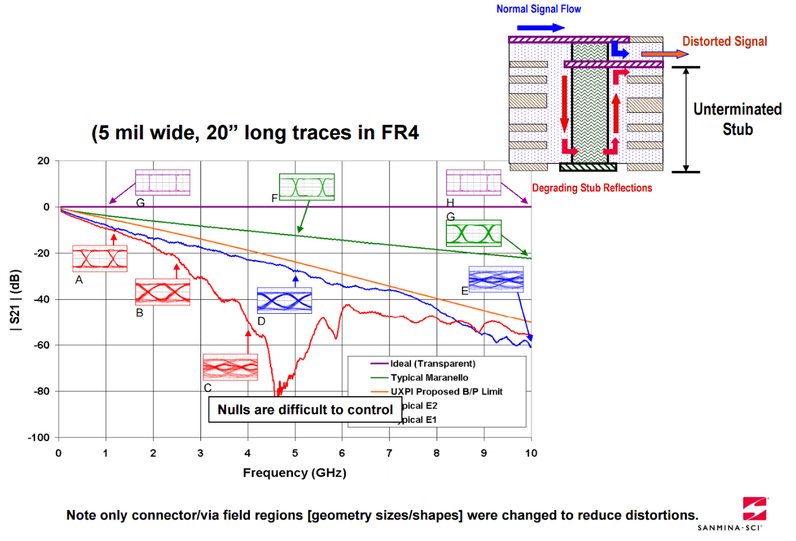
Signal distortion caused by stub
Back drilling has been widely recognized as a simple and effective method to minimize signal attenuation caused by via stubs. Back drilling, also known as fixed-depth drilling, uses a CNC drilling machine to remove the stub sections of vias.
The drill bit diameter used in back drilling is typically 8 mils larger than the via diameter to facilitate the removal of unnecessary conductive stubs. To ensure that back drilling does not penetrate nearby traces and planes, the distance between traces and planes near the via and the corresponding layer of the back-drilled hole should be at least 10 mils.
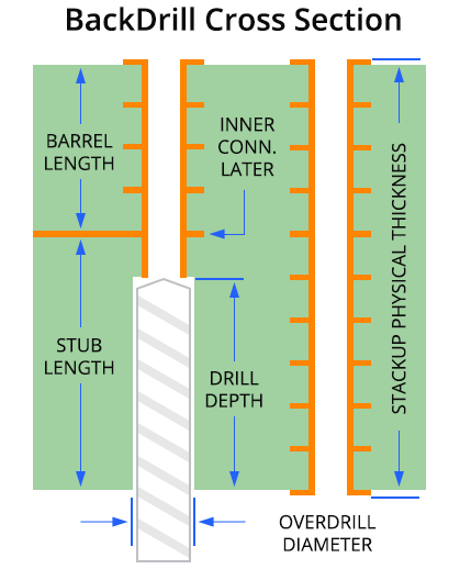
Cross-section diagram of back drill
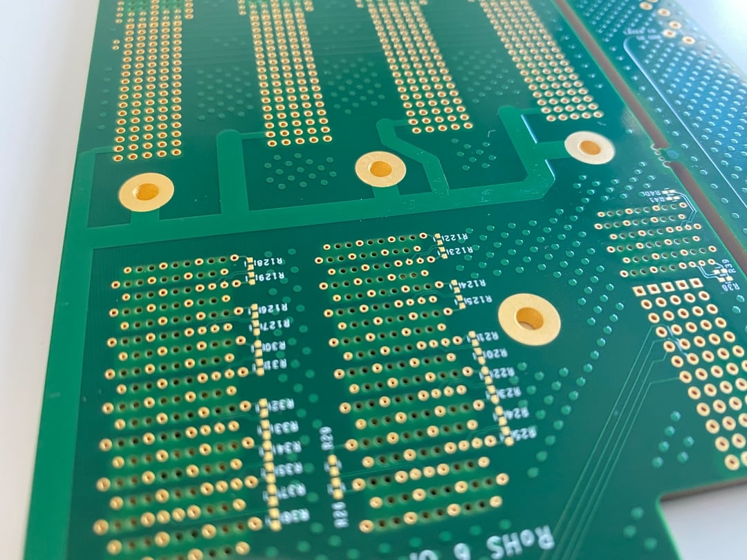
Backboard PCB with back drilling completed
Note: The above content is collated from the Internet, and the copyright belongs to the original author. If there is any infringement, please contact us for deletion.