
Sunshine is committed to technology development.
Our CTO David Aldape has over 25 years of industry experience, and leads a dedicated team of R&D engineers.
Development projects for 2016-2017:
Increase Plating Aspect Ratio to 30:1 or higher
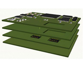
Backplane capability;large format and very thick boards
Reduce controlled impedance to lerance of ±5% or less
Introduction of advanced plating and photo lithography methods
Advanced tooling systems for improving L2L registration
Continual addition of new materials for HDI, High Speed/Low Loss,thinnerstructures and sub‐assemblies applications (for example: ZETA®,I‐Tera®,I‐Speed®,Tachyon G100®, Megtron 7, and EMC 828&888K)
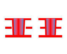
Deep Microvias (L1‐L3, Aspect Ratio 1:1 or greater)
Thermal Management Solutions: Metal Core, Conductive Paste (Ormet and Tatsuta)
Embedded Component PCBs.
Provide additional routing density、Improved Impedance Performance、 RF Micro Via Solutions、Solid Copper Plated Surface for BGAs、 Improved Current Carrying Capacity
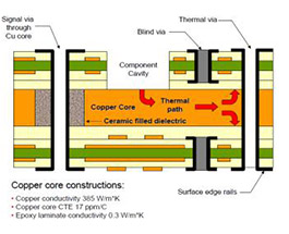
Thermal Management 、Improved Heat Distribution 、 Increased Thermal Conductivity、Copper core CTE 17ppm/C 、 Thermal Conductivity 385 WmK
Buried internal resistors 、Aerospace, Telecommunications、Micro Wave and Medical 、Flexable circuit heaters
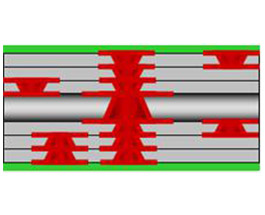
All layer via maximizes design freedom、 Solid Copper provides better reliability、 Superior Electrical characteristics
Buried resistors and printed internal resistors 、Buried capacitors and dielectric insulators 、 Planar convertors and transformers 、 Embedded semiconductors and thin dies、 Flex-rigid embedded components
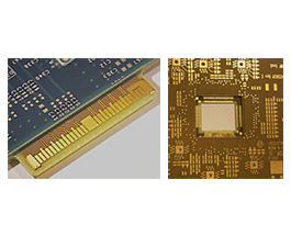
Recessed Chips for Gold Wire Bonding 、 Connectors with limited thickness
 WeChat
