AI accelerator cards using GPUs or xPUs will soon transition from 7nm and 5nm processes to the 3nm process node. With the continuous improvement of process technology, the core operating voltage of xPUs is also decreasing, with the current nominal core voltage ranging between 0.75V and 0.9V. When AI accelerator cards are processing model training computations, the core may require currents ranging from 600 to 1800A. As the current increases, the losses and PDN (Power Distribution Network) issues caused by PCB trace impedance become quite challenging.

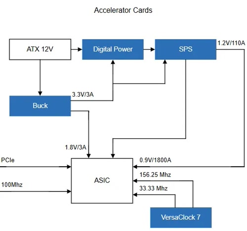
Power Architecture of AI Accelerator Cards
The source of the image is Renesas
Change in Power Layout
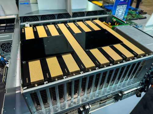
To improve computational density, AI accelerator cards using PCIe interfaces are typically installed in clusters within servers, with 4 or 8 accelerator cards installed in each AI server. This significantly compresses the lateral power transmission path. Considering the noise of high-current switching power supplies on high-speed signals, multiple switching power supplies can only be moved closer to the core. Faced with the 600-1800A high-current demand of the xPU core voltage, the traditional multiphase buck power supply solution is almost unable to meet the requirements.

NVIDIA H200 NVL 4 GPU cluster
Dynamic Response of Power Supply
The transient power of AI accelerator cards may reach twice or even more than the rated maximum power. Under such conditions of significant current transient changes, it is also necessary to ensure that the xPU voltage supply voltage is not too low to cause the system to hang or too high to damage the xPU. This requires extremely high standards for power supply tolerance, ripple, and load transient response.
I2R Losses and Thermal Management in Long Power Path Tracing
Thermal management is also one of the major challenges faced. The traditional power supply method places the voltage regulator on one side of the xPU, with current transferred laterally to the processor. Since the current is not large, the voltage (I2R) drop caused is within an acceptable range. However, when the current reaches 600-1800A, the voltage drop on the PCB power layer transmission path will increase exponentially, and even a few centimeters of PCB power tracing will generate a large amount of loss.
Vertical Power Supply Solution for AI Accelerator Cards
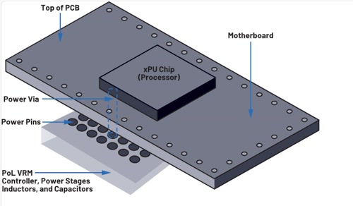
For AI accelerator card clusters, vertical power supply is the best solution. In the vertical power supply solution, the power module is directly installed below the other side of the processor PCB. At this time, the distance of current transmission is the thickness of the PCB. Compared with lateral power supply, it greatly shortens the distance that current passes through the motherboard, greatly reducing the impact of transmission path parasitic parameters on power quality, and the power transmission loss can be reduced by up to 95%.

Vertical Power Supply Schematic
The source of the image is Analog
Change in the Position of High-Frequency Capacitors under the Vertical Power Supply Solution
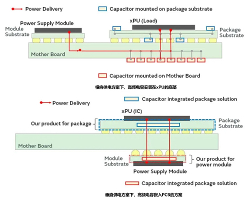
In the lateral power supply solution, many high-frequency capacitors are placed directly below the xPU. These low ESR capacitors can more effectively filter out high-frequency noise, reduce power ripple, provide transient current, and improve the response speed of the power supply.
Under the vertical power supply solution, the position where high-frequency capacitors were previously installed needs to be replaced with a power module. The position of the high-frequency capacitors will change. One solution is to integrate the high-frequency capacitors into the power module, but this solution is too far from the power supply pins for the high-frequency capacitors. The ideal solution is to embed the capacitors into the substrate of the xPU and the PCB of the power module respectively.

Changes in the Position of High-Frequency Capacitors
The source of the image is Murata