
With the continuous expansion of microwave and radio frequency technology applications, more and more electronic devices are being designed and applied in the microwave band (>1GHZ) and even in the millimeter wave band (77GHZ). For example, the automotive radar uses a 77GHz millimeter wave antenna.

Tesla millimeter-wave radar PCB
In general, high-frequency PCBs are defined as PCBs with electromagnetic frequencies above 1 GHz.
As the frequency of signals on PCBs increases, the performance requirements for PCB materials also increase. The materials need to have excellent electrical properties, good chemical stability, and very low loss on PCBs as the frequency of signals increases.
RF transmission lines are media that transmit RF power from a source to a load through structured paths. These transmission lines need to follow certain routing rules to achieve minimum loss from the source to the load. On PCBs, two of the most commonly used and cost-effective transmission lines are microstrip and coplanar waveguide (CPWG).
In both transmission lines, part of the electromagnetic field exists in the air, while the other part exists in the substrate. The dielectric constant of air is 1, while the dielectric constant of the substrate is greater than 1. Therefore, the effective dielectric constant of the transmission line is less than the dielectric constant of the substrate itself.
Microstrip lines run on the top layer of a PCB and have RF signal lines on top and a ground plane below. Here's a cross-section of a microstrip line.Factors that affect the characteristic impedance of a microstrip line include:
▪ Substrate height (H)
▪ Dielectric constant of the substrate (εr)
▪ Line width (W)
▪ Copper thickness (T) for the RF trace

The construction and processing of microstrip lines are both simple. For a given sheet material, the effective dielectric constant of microstrip lines is greater than that of coplanar waveguides. Compared to coplanar waveguides, the layout is also relatively compact.
CPWG is similar to microstrip, but it has a grounding on either side of the RF trace.

The characteristic impedance of CPWG depends on the following factors:
▪ Substrate height (H)
▪ Dielectric constant of the substrate (εr)
▪ Line width (W)
▪ Gap between the RF trace and the grounding (G)
▪ Copper thickness (T) for the RF trace
CPWG has advantages over microstrip lines in the following aspects:
▪ Provides better isolation and EMI performance for RF traces
▪ Easier grounding for shunt components on the RF trace
▪ Reduces crosstalk with other signal lines
▪ Lower loss at high frequencies
▪ Ensure that the RF trace has a characteristic impedance of 50 ohms, whether using microstrip or CPWG. Use an impedance calculator to calculate the specific parameters for the characteristic impedance trace.
▪ The characteristic impedance of the entire RF trace must remain constant, and the width of the RF trace needs to be maintained constant. For CPWG, the spacing between the RF trace and the grounding needs to be maintained constant.
▪ For CPWG, ensure that the gap between the RF trace and the grounding is less than the height of the substrate to the reference ground. Otherwise, the RF trace will behave as a microstrip line.
▪ For CPWG, ensure that the grounding trace width for the RF grounding is wider than the gap between the RF trace and the grounding.
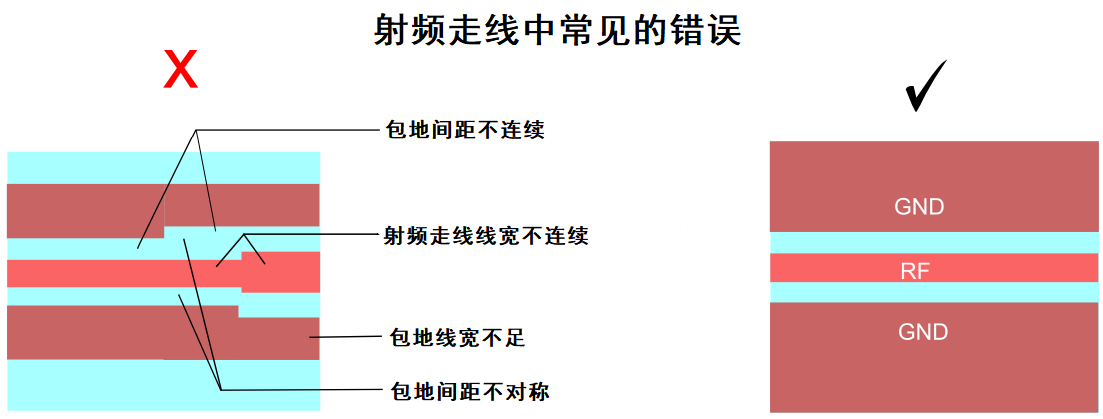
▪ Ensure that there is a clean and complete reference ground plane under the RF wiring, and that the RF wiring cannot cross other wiring or span the ground plane to ensure that the correct return path is provided for the RF current.
▪ The length of the RF wiring should be as short as possible, as the attenuation of the RF signal is proportional to the length of the wiring.
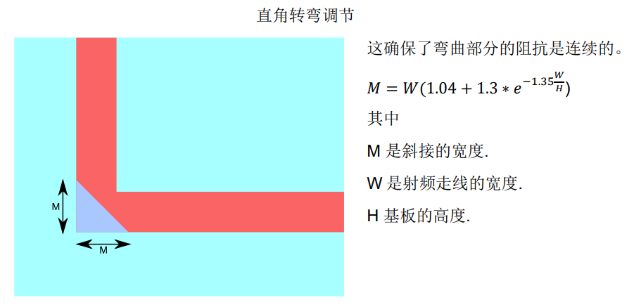
▪ Avoid bending RF traces. If unavoidable, use curved lines to bend them, rather than sharp bends, to maintain uniform trace width. For right-angle turns, adjustments are required, as shown in blow.
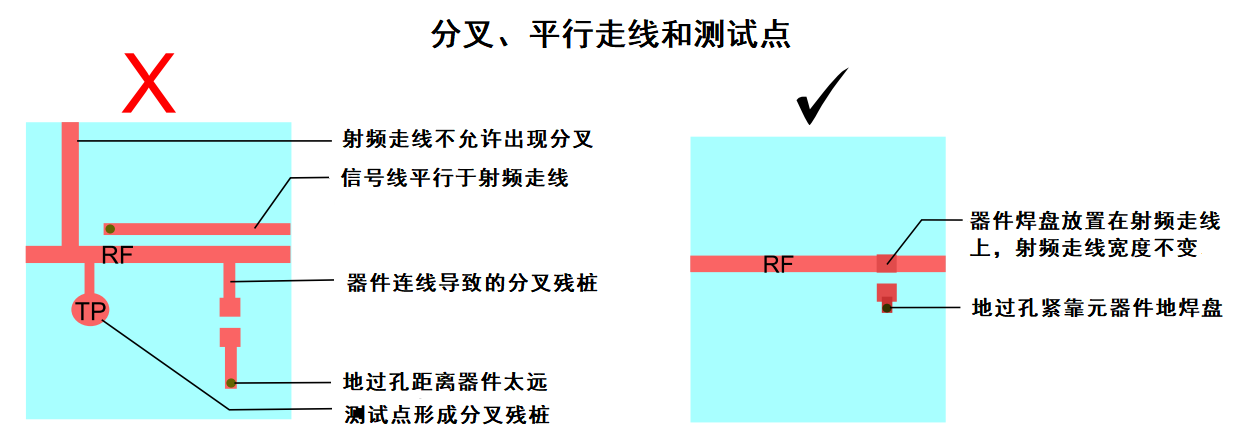
▪ Avoid branch points in the RF trace, as they can affect impedance matching. Layout components on the RF trace while following reference designs, and avoid branch points that may result from component placement.
▪ Do not place any other traces near or parallel to the RF trace to avoid signal coupling.
▪ Do not place test points on the RF trace, as they can affect impedance matching.
The four-layer PCB can provide a complete ground plane and power plane, making routing of signal lines simpler.
top:RF IC and components, antenna
2nd:ground plane
3rd:Power layer
bottom: Non-RF components and signals
Complete power supply layer and ground plane, convenient decoupling capacitor grounding, lower voltage drop of power PDN network.
The 50 ohm characteristic impedance needs to be adjusted during processing with the board parameters provided by the PCB manufacturer to ensure that the final manufactured PCB meets design requirements.
When cost sensitivity is a concern, a two-layer board is often chosen. If a two-layer board is chosen, the substrate thickness should be kept as thin as possible, as the RF trace width is directly proportional to the substrate height for a characteristic impedance of 50 ohms. Thicker PCBs (> 0.8mm) will result in wider RF traces, which can crowd out space for other signal traces. Additionally, wider RF traces can trigger the generation of spurious parasitic waves.
Top layer:All ICs and RF lines
Bottom layer:Ground plane
If a complete ground plane cannot be achieved on the bottom layer, it is important to ensure that there is a continuous ground plane under the RF circuitry.
In RF circuit design, the ground plane is very important. The return path of the RF signal is located on the ground plane under the RF trace. To achieve good RF performance, the return path needs to be continuous and as wide as possible. If the ground plane is interrupted, the return current will seek the next minimum return path around the interruption. This increases parasitic inductance, affecting impedance matching between the RF trace and antenna, and significantly attenuating the RF signal. Additionally, if the ground layer under the RF trace is narrow and does not meet the requirements of a microstrip line, it can also cause significant attenuation of the RF signal.
Ground plane considerations:
▪ Do not have any wiring above the RF trace on the ground plane, even on a double-layer PCB, it is best to use one layer exclusively for grounding.
▪ Paste copper and ground vias in the un-routed areas of the top and bottom layers, ensuring that the via spacing does not exceed one-twenty-fifth of the signal wavelength.
▪ Do not use a double-layer PCB when using CSP packaged chips, as the signal needs to pass through the second layer to exit, making it difficult for the RF signal to have an uninterrupted ground plane.
▪ The ground layer under the RF trace needs to be spacious.
▪ The ground planes on different layers need to be closely connected using vias to form a good ground throughout the PCB, achieving shielding effects.
▪ The power layer should be contracted with the ground plane, and it is best to envelope the power layer with ground and connect them through vias to reduce radiation from switching power supplies.
The production process of high-frequency and high-speed PCB boards is basically the same as that of ordinary PCB boards, and the key point of performance difference lies in the characteristic parameters of the board material.
Dk is the abbreviation of Dielectric constant, which is a coefficient representing the insulating properties and is represented by the letter ε. The transmission rate of signals is inversely proportional to the square root of the dielectric constant of the material, and a high dielectric constant can easily cause signal transmission delays. Generally speaking, the smaller the better.
Df is the abbreviation of Dissipation factor, which is also known as dielectric loss factor or loss tangent (tanδ). It is the ratio of the loss modulus to the storage modulus of a material. It affects the quality of signal transmission, with lower dielectric loss resulting in lower signal loss.
The most widely used substrate material in the PCB industry is epoxy resin fiberglass cloth copper clad laminate FR-4, which consists of one or multiple layers of fiberglass cloth impregnated with epoxy resin. It has low cost and electrical and mechanical properties suitable for a variety of applications.
The dielectric constant of FR-4 is as high as 4.2-4.8, and the dielectric loss factor is greater than 0.0015, making it difficult to meet the requirements for reliability, complexity, electrical performance, and assembly performance of high-frequency and high-speed PCB products.
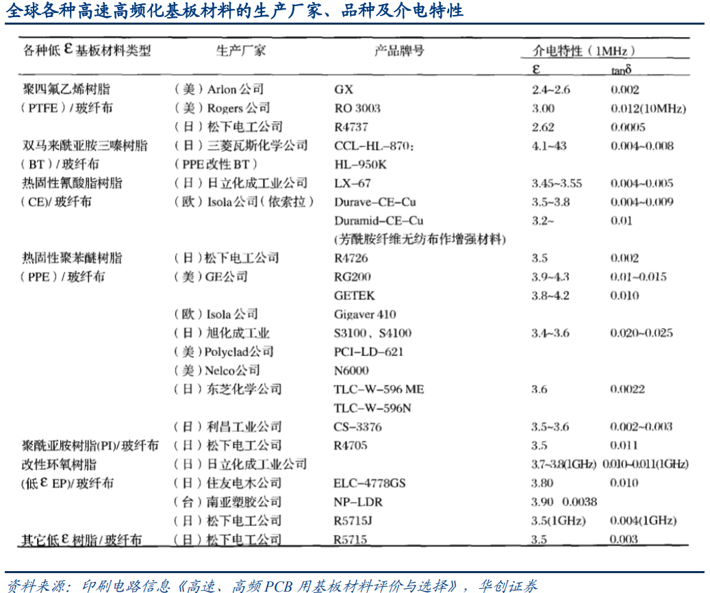
Under the current trend of high-speed and high-frequency, the more mainstream PCB materials include polytetrafluoroethylene resin (PTFE), epoxy resin (EP), bismaleimide triazine resin (BT), thermosetting cyanate ester resin (CE), thermosetting polyphenylene ether resin (PPE) and polyimide resin (PI), which lead to more than 130 types of copper clad laminates. Their common characteristics are that the dielectric constant and dielectric loss factor are very low or low.
In addition to dielectric constant and dielectric loss factor, resin materials with low CTE (higher dimensional stability) and high Tg (high heat resistance/high temperature modulus retention) are more popular.
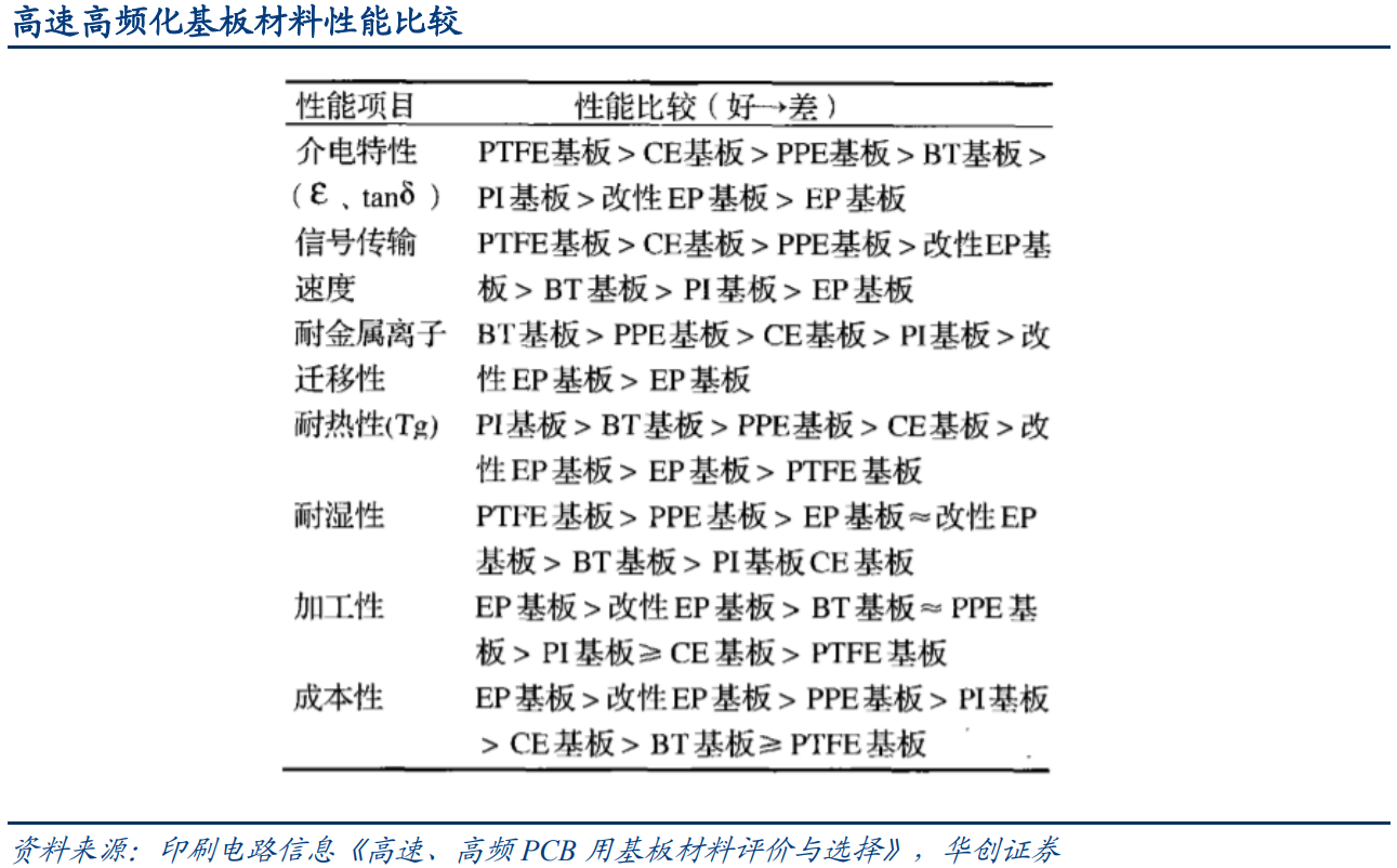
For high-frequency PCBs, the most important indicators are dielectric properties, signal transmission speed, and heat resistance. PTFE substrates have the best performance in the first two areas and are the most suitable resin material for high-frequency PCBs.
Article reference source:天线设计和射频布局指南-AN91445 Cypress。5G 材料环节核心受益标的,基站高频 PCB 板和手机天线 FPC 基材国内龙头-华创证券。
Note: The above content is collated from the Internet, and the copyright belongs to the original author. If there is any infringement, please contact us for deletion.