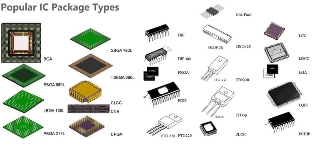
What is chip packaging?
Chip packaging technology mainly includes: DIP dual in-line package, component package, PGA pin grid, BGA ball grid array (PBGA substrate, CBGA substrate, FCBGA substrate, TBGA substrate, CDPBGA substrate), CSP package (traditional lead frame form, rigid interposer type, soft interposer type, wafer size package), MCM package, etc.

Traditional packaging methods mainly connect the bonding pads of the wafer to the pins of the substrate based on wires to achieve electrical connectivity, and finally cover with a housing to form protection. The main methods include DIP, SOP, QFP, and so on.
In the industry trend of chip manufacturing approaching the limit of silicon chips and Moore's Law slowing down, the emergence of advanced packaging optimizes the connection between bare chips, effectively shortening the signal distance between dies under heterogeneous integration architecture, resulting in performance and power consumption optimization.
At present, the advanced semiconductor packaging technologies in the industry mainly include SiP, WL-CSP, FC, eWLB, PiP, PoP, and 2.5D/3D packaging technologies.
IC carrier board is the core component of chip packaging

IC carrier boards have higher technical requirements than PCBs. IC carrier boards are developed from HDI technology, and the processing accuracy gradually increases from ordinary PCBs to HDI to SLP (similar carrier boards) to IC carrier boards. IC carrier boards currently use Tenting (PCB subtractive method), SAP (semi-additive method), and MSAP (modified semi-additive method) processes for manufacturing, requiring different equipment, higher processing costs, and more refined indicators such as line width/line spacing, board thickness, and aperture. At the same time, they also have higher heat resistance requirements.
IC carrier boards can be divided into four categories according to mainstream packaging methods: WB/FC×BGA/CSP
WB/FC is the connection method between bare chips and carrier boards.
Wire Bonding (WB) uses wire leads to connect bare chips to carrier boards, while Flip Chip (FC) turns the front of the bare chip upside down and directly connects it to the carrier board with solder bumps, serving as a buffer interface for electrical connection and transmission between the chip and the circuit board.
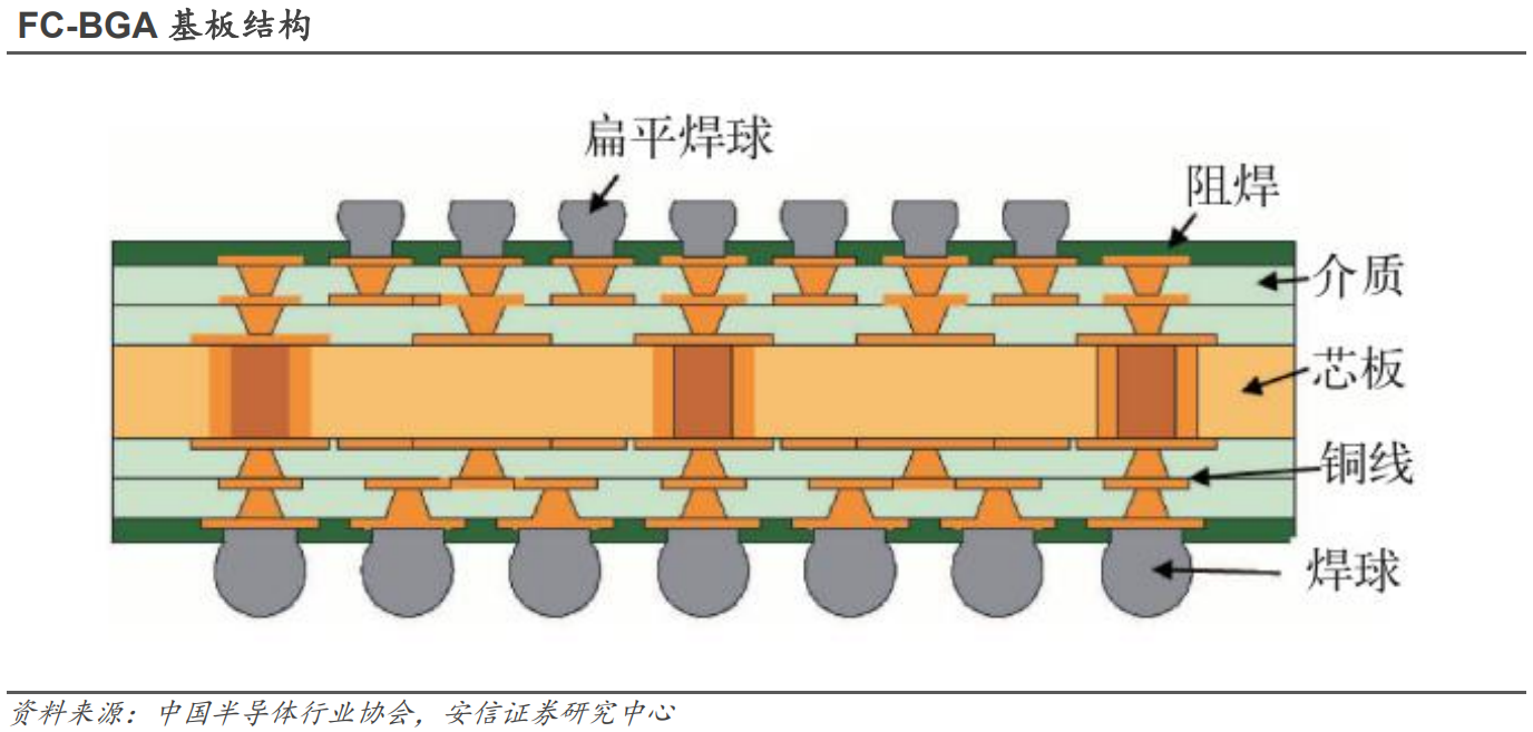
FC uses solder balls instead of leads, which improves the signal density of the carrier board compared to WB, improves chip performance, facilitates bump alignment correction, and increases yield. It is a more advanced connection method.

Wire Bonding 与 Flip Chip
BGA/CSP is a connection method between the carrier board and the PCB.
CSP is suitable for mobile-end chips with small size and high density, while BGA is suitable for PC/server-level high-performance processors.
BGA (Ball Grid Array) is a packaging method that arranges many solder balls in an array on the bottom of a chip, replacing traditional metal lead frames with solder ball arrays as the pins.
CSP (Chip Scale Package) can make the ratio of chip area to package area exceed 1:1.14, which is quite close to the ideal case of 1:1. It is about 1/3 of the ordinary BGA, which can be understood as a BGA with smaller solder ball spacing and diameter.

BGA VS CSP

The substrate of IC carrier board is similar to PCB copper clad laminate, which is mainly divided into three categories: rigid substrate, flexible film substrate, and co-fired ceramic substrate. Among them, rigid substrate and flexible substrate basically occupy the entire market space, so here we mainly focus on rigid substrate.
IC rigid carrier boards are divided into three categories based on substrate materials: BT/ABF/MIS.
BT substrate is a resin material developed by Mitsubishi Gas Chemical. Its good heat resistance and electrical properties have made it a replacement for traditional ceramic substrates. It is not prone to thermal expansion and contraction, has stable dimensions, and has a hard material and thick lines. It is mainly used for mobile phone MEMS, communication, and storage chip packaging.
ABF is a multi-layered thin film material developed by Ajinomoto of Japan. It has higher hardness, thinner thickness, and good insulation properties, making it suitable for IC packaging with fine lines, high layers, multiple pins, and high information transmission. It is used in high-performance CPU, GPU and other fields.
MIS is a new type of material that is different from traditional substrates. It includes one or more pre-encapsulated structures that are interconnected by electroplating copper. The lines are finer, the electrical performance is better, and the volume is smaller. It has rapid development in the field of power and analog ICs.

NVIDIA GH200 uses ABF carrier board
The development of IC carrier board
Technological Trends
The development of packaging technology drives the development of carrier boards. The FC process has become mainstream, and multi-chip 3D packaging and large-size high-density multi-layer substrates are the current development direction. In order to improve performance, reduce power consumption, and improve I/O, single-chip packaging at this stage will gradually develop towards multi-chip or integrated chip packaging. 3D packaging is also the development direction of next-generation substrates for high-density bumping and high-rigidity requirements of substrates.
Market Trend
The 5G ecosystem is expected to become the core driving force leading the demand for packaging market.
In the 5G era, the demand for high-performance, small-sized, and low-power electronic products and chips is increasing. According to semiconductor industry observation, 5G mobile phones receiving high-frequency bands rely on complex RF front-end and antenna designs. Through advanced packaging technology, antennas can be embedded into end products to improve transmission speed and meet users' needs for lightweight and portable, fast transmission, excellent performance, and low energy consumption. According to Yole data, the global 5G smartphone packaging market size will reach US$2.6 billion in 2026, with a CAGR of 31%.
In the era of AI computing power, the demand for IC carrier boards is increasing.
Large models such as ChatGPT have huge parameters, and the training and reasoning processes require a large amount of computing power chips. The potential market for AI accelerators in data centers will grow from 30billionthisyeartomorethan150 billion in 2027. AI chips mainly include GPUs, CPUs, FPGAs, and ASICs.
Chiplet technology injects new vitality into the industry.
In the post-Moore era, the improvement of economic efficiency has reached a bottleneck, and the importance of advanced packaging in the process of improving chip integration, electrical connectivity, and performance optimization has gradually become prominent. Chiplet ("core particle") technology has emerged as the times require.
Chiplet is a system-on-chip (SoC) that integrates multiple functional chips into a single package through internal interconnection technology. It can package chips with different manufacturing processes together to achieve optimal system performance, improve chip yield, reduce design complexity and cost, and reduce manufacturing costs.

Chiplet packaging
According to Omdia's statistics, the global market size of processor chips using Chiplet will reach 5.8billionin2024and57 billion by 2035, with a compound annual growth rate of about 23.09%. At the same time, the rapid growth of the market size of Chiplet processor chips will drive the demand for ABF carrier boards.
Note: The above content is collated from the Internet, and the copyright belongs to the original author. If there is any infringement, please contact us for deletion.