
Why should we pay attention to Mini LED?
Small-pitch LED display is accelerating the replacement of traditional display
Generally, it is considered that only the LED with a dot pitch within 2.5mm can be called a small-pitch LED. The LED screen consists of lamp beads, and the distance between the center points of two lamp beads is called the dot pitch. The LED display industry generally uses the dot pitch to define product specifications, such as P10 refers to a pixel pitch of 10mm. The smaller the dot pitch, the higher the pixel density (PPI) of the LED display screen, and the better the display resolution and imaging effect.
The performance advantages of small-pitch LED display are obvious, forming a trend of replacing traditional display technology. Small-pitch LED screens have seamless splicing, adjustable high brightness range, high color reproduction, good display uniformity and consistency, low energy consumption and long life, which are not available in LCD splicing screens and DLP splicing screens. In recent years, small-pitch LEDs have gradually moved from outdoor to indoor, forming a trend of replacing DLP and LCD splicing screens.
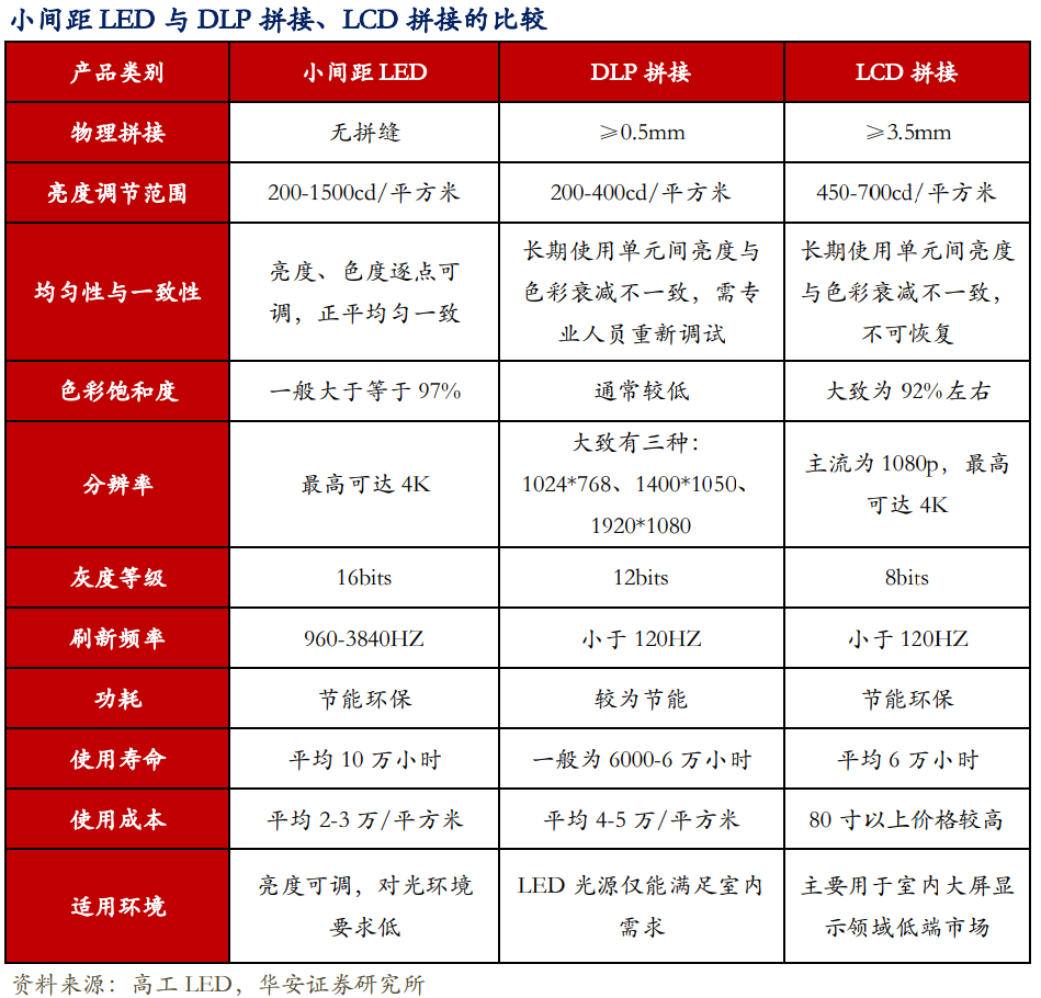
Airports, shopping malls, schools, enterprises, exhibitions and other markets have begun to use small-pitch LEDs to display various types of information. The application of new LED technology will accelerate the penetration of small-pitch in the commercial field, forming a trend of replacing traditional splicing screens.
Compared with traditional small pitch, Mini LED uses smaller LEDs to form a high-density LED array, which can be used as an LCD backlight for large-size displays, smartphones, automotive panels, laptops, and other products. It can also use RGB three-color LEDs to achieve self-emission display.
Evolution of LED technology
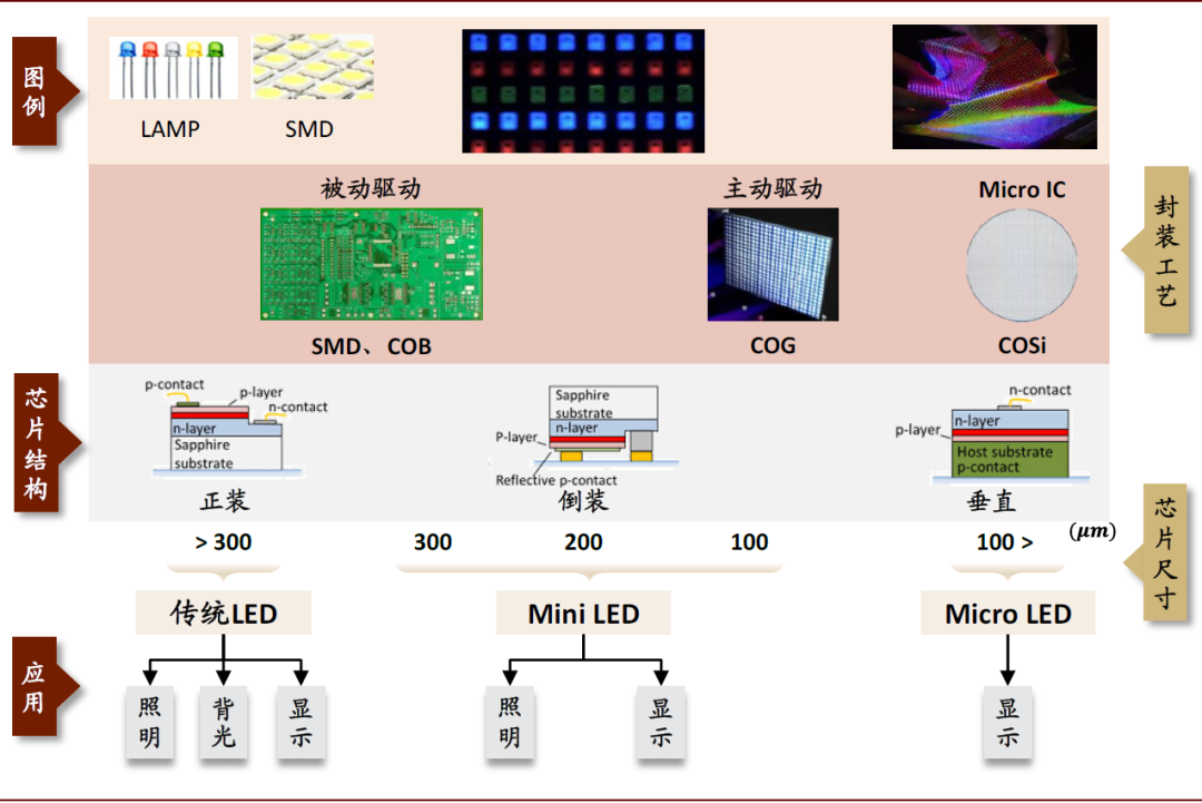
Mini LED backlit TVs can provide high brightness levels similar to LCD TVs, pure dark fields similar to OLED TVs, the ultimate contrast and dynamic range, color performance, and dark detail through precise control of the backlight brightness in different zones. Combining the advantages of LCD and OLED, they present a near-realistic picture and immersive feel on the TV screen, and are more affordable.
Mini RGB LED direct display not only inherits the advantages of high brightness, high reliability, and fast response speed of small-pitch display, but also has the characteristic of self-illumination without backlight, which can achieve the effect of small size, thinness, and more delicate display effect. At the same time, it is more energy-efficient and cost-effective than other display technologies. Mini LED display is mainly used in high-end commercial display. With the popularity of 2K/4K high-definition video, Mini LED display has great potential in the field of commercial display in the future.
Mini LED has two definitions. In a broad sense, it refers to LED lamp beads with pixel pitch less than P1.0, which can be achieved using traditional SMD surface-mount packaging, IMD hybrid packaging, and positive chip COB packaging. In a strict definition, Mini LED requires the size of the packaged LED to be between 50-200um, which can only be achieved using flip chip technology.
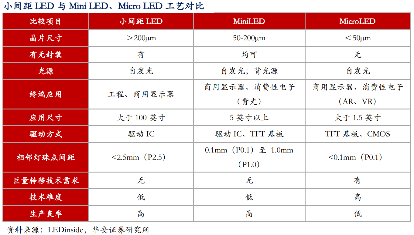
The key to high-density integration of LEDs lies in packaging
Mini LED is facing new technical challenges in various aspects such as materials, equipment, chips, driver ICs, PCB design, and packaging during the continuous shrinkage of crystal size. From the perspective of technology itself, the main issues are yield, efficiency, consistency, and reliability, especially the packaging process.
The display screen has extremely high requirements for image quality and display effect, and different processing techniques for the encapsulation surface, as well as light color differences between pixels, can easily lead to problems such as inconsistent light mixing and difficult calibration, which in turn affect the display effect. Since the development of the LED display industry, in addition to the traditional direct insertion process, a variety of packaging processes including SMD, COB, IMD, etc. have been formed.
The mainstream packaging technology in the small pitch market - SMD process
SMD is short for Surface Mounted Devices. LED packaging plants using SMD process fix the bare chip on the bracket, electrically connect them through gold wire, and finally protect them with epoxy resin. The SMD-packaged lamp beads are handed over to display manufacturers, and are soldered through reflow soldering to form a module for assembly. SMD uses surface mount technology (SMT), which is highly automated and has the advantages of small size, large scattering angle, good luminous uniformity, and high reliability.
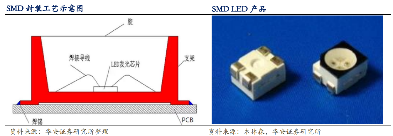
However, as SMD devices become smaller, the soldering area on the lamp panel also shrinks sharply, which greatly increases the requirements for SMT patching processes, and at the same time greatly affects the production efficiency of manufacturers.
For example, a P1.5 product requires 440,000 lights per square meter, while a P1.0 product requires 1 million lights per square meter. Not only has the number of SMT patches increased by approximately 2.3 times, but the SMT patching speed also needs to be significantly reduced, greatly affecting production efficiency.
The current market is developing rapidly, with a trend towards miniaturization of small-pitch LEDs, and SMD surface-mount packaging is facing technological bottlenecks, making it difficult to play a role in the field of smaller pitch.
Effectively solve the high-density packaging-COB process
COB, or Chip on Board, is a packaging technology that uses a thermal conductive epoxy resin (silver-doped epoxy resin) to cover the silicon chip placement points on the substrate surface, and then uses conductive or non-conductive adhesives to adhere the LED chip to the interconnection substrate through adhesive or solder. Finally, the chip is electrically interconnected with the PCB board through wire bonding (gold wire).
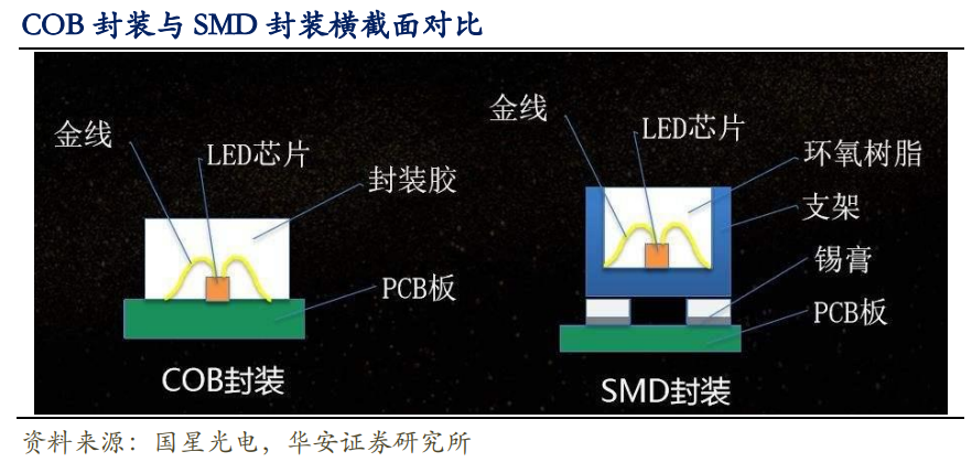
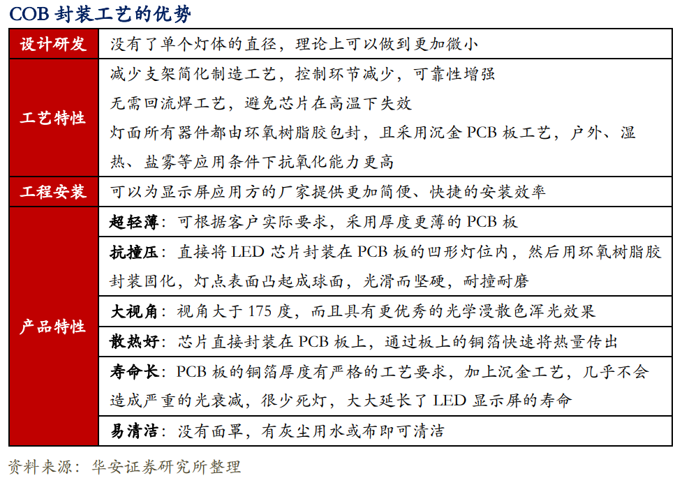
Compared to SMD packaging, the small pitch of COB packaging has the characteristic of "the smaller the density, the more obvious the advantages (in terms of thinness, impact resistance, flexibility, good display quality, moisture resistance, and shock resistance)".
Combination of economy and technology - IMD process
Currently, besides COB packaging technology, the mainstream technology of small-pitch packaging on the market is IMD integrated packaging technology, which integrates two or more pixel structures into one packaging unit. Currently, the four-in-one technology is the most mature application.
The IMD process still uses surface-mount technology, combining the advantages of SMD and COB. From the pixel structure point of view, traditional SMD packaging is basically one pixel; COB packaging is to directly package the LED chip onto the module substrate, and then mold each large unit as a whole. A packaging structure has hundreds or thousands of pixel points. The "four-in-one" of IMD is a "lamp bead" composed of four RGB-LEDs in one packaging structure. IMD continues to use mature sorting technology with small pitch in sorting, which can carefully select the wavelength and brightness of the device, and the devices from different molds are evenly dispersed before taping, effectively avoiding local color differences caused by subtle differences during packaging, resulting in better color consistency.
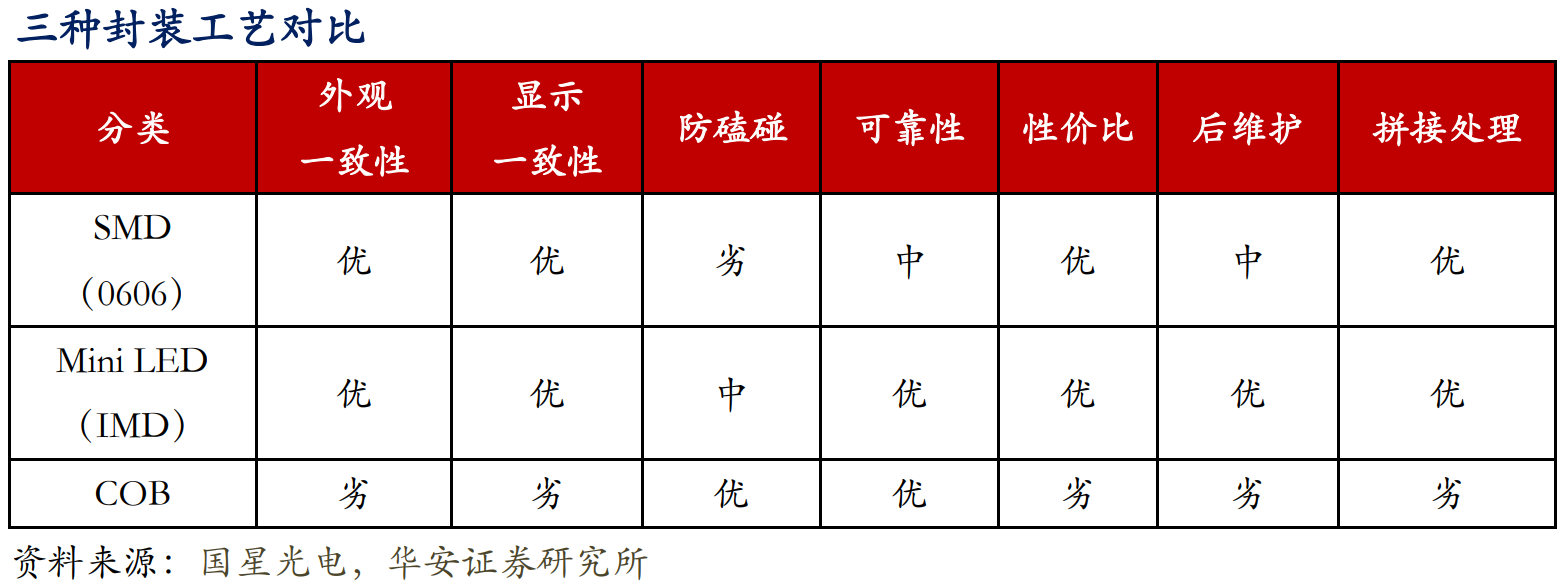
The difference of PCB required for different LED packages
Take the LED screen with P0.9 for example
Generally, the PCB of COB-P0.9 is 8 layers and 3 levels.
Because the lamp bead itself has been integrated with circuits, the IMD-M09T only requires 8 pins for 4 pixels, which increases the PCB wiring space of the screen factory by 50%. Customers using the IMD-M09T typically only require 6 layers of 2-stage PCBs, which is more than 20% cheaper.
SMD also requires an 8-layer 3-stage PCB board, but the accuracy requirements are not as high as COB.
Note: The above content is collated from the Internet, and the copyright belongs to the original author. If there is any infringement, please contact us for deletion.