AI server products, as a key component of artificial intelligence, have experienced rapid development in recent years. From the hardware architecture perspective, AI servers are typically equipped with high-performance central processing units (CPUs), graphics processing units (GPUs), tensor processing units (TPUs), or dedicated AI computing chips, along with large amounts of memory and storage space.
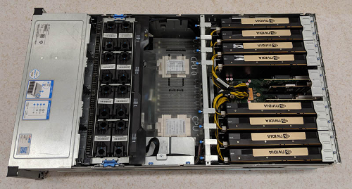
In terms of heterogeneous architecture, AI servers can be categorized as CPU+GPU, CPU+FPGA, CPU+TPU, CPU+ASIC, or CPU+multiple accelerator cards. Currently, the most common configuration in products is CPU+multiple GPUs.

GPU accelerator card clusters in AI servers
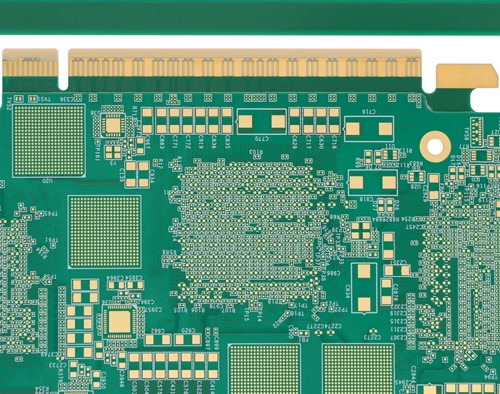
Against the backdrop of rapid development in the AI server market, AI server accelerator card modules are becoming increasingly integrated, with denser blind via stacking leading to higher PCB order numbers. Since the AI accelerator card gold finger area needs to meet PCIe 5.0 protocol standard requirements, this means the gold finger thickness is fixed. Due to the high layer count of AI accelerator cards, the PCB thickness exceeds the gold finger thickness, requiring the design of embedded inner layer fingers that are later exposed through a uncovering process, significantly increasing PCB manufacturing complexity.
As AI accelerator cards integrate multiple GPUs, PCB design will shift toward higher layer counts, high-density BGAs, and high-impedance transmission speeds. PCBs will require higher-grade high-speed materials and ultra-low roughness copper foil. These requirements for AI accelerator cards will drive the PCB industry into a new stage of development.
AI Accelerator Card PCB Characteristics
The 26-layer PCB product features for AI accelerator cards produced by Sunshine are as follows:
High-Speed Materials
The PCB adopts M7-grade materials, which can meet current AI accelerator card requirements for signal loss during high-speed signal transmission.
High Layer Count, Thick Board, Large Size
AI accelerator cards typically consist of multiple GPU chips. As the number of large-size BGA chips increases, the entire board's routing interconnections become denser, corresponding to increased PCB layer count, board thickness, and size.
Multi-Order Blind Via Technology
Through multi-order blind via technology, PCB layer count and board thickness can be effectively reduced, avoiding unnecessary stubs and improving signal transmission integrity.
High Aspect Ratio
With higher-density routing designs, via hole diameters also decrease. As board thickness increases, the PCB's aspect ratio becomes larger.
Inner Layer Uncovering Gold Fingers
Since gold finger thickness must meet PCIe protocol requirements, but GPU integration density increases make PCB board thickness inconsistent with required gold finger thickness. Therefore, only through inner layer uncovering design can embedded fingers be manufactured in advance and then exposed in the finished product.
AI Accelerator Card PCB Manufacturing Technical Challenges
Stack-up Design Challenges
AI accelerator cards adopt 7-order HDI design with embedded uncovering gold fingers in inner layers. Seven pressings exceed conventional FR4 copper-clad laminate pressing limits. If stack-up design is unreasonable and material expansion/contraction control is insufficient during pressing, finished PCBs will exhibit warpage, bowing, and other issues, preventing component mounting.
High Multi-layer Pressing Challenges
AI accelerator cards use M7-grade materials, which have significantly different pressing parameters from conventional FR4 materials. During M7-grade material pressing manufacturing, the following issues frequently occur:
Multiple pressings create multiple fusion or riveting areas at board edges, forming local height differences that easily lead to pressure loss.
Multiple pressings make it difficult to achieve stable expansion/contraction patterns due to different residual copper rates and material expansion/contraction stability challenges across layers.
Multiple pressings require PP dehumidification, sub-board browning pre-baking, pressing program adjustments, and control of residence time from browning to pressing. Improper handling can easily lead to delamination and bursting.
Multi-order HDI with different thickness core boards requires high pressing alignment accuracy and board thickness uniformity requirements. One pressing's alignment accuracy directly affects subsequent HDI stacking alignment manufacturing.
Considering these factors, abnormalities in expansion/contraction, parameters, or manufacturing process design will directly lead to product quality issues such as delamination, bursting, inner layer short circuits, and expansion/contraction abnormalities.
Pattern Alignment Control Challenges
This AI accelerator card has a large single SET size. For high multi-layer alignment requirements and BGA line embedding, dense BGA hole-to-line spacing is typically only 5mil or even smaller. Meanwhile, HDI laser hole diameters are typically designed at 0.1-0.125mm with single-sided ring width of 2.5-3mil, making pattern alignment accuracy requirements extremely challenging. Multiple pressings require high pattern alignment accuracy, with the following issues typically increasing manufacturing difficulty:
Buried hole and laser drilling alignment requires ±2mil accuracy, making manufacturing extremely difficult.
HDI laser holes with 2-3mil single-sided ring width make consistency between laser drilling and pattern alignment challenging.
Expansion/contraction differences create difficulties for drilling and pattern manufacturing.
Inner Layer Gold Finger Uncovering Challenges
Since the designed board thickness far exceeds gold finger thickness requirements, fingers must be manufactured as embedded fingers and then exposed through uncovering to complete finger manufacturing. This process typically presents the following challenges:
Embedded finger layers require gold plating, with complex, troublesome, and difficult processes, making finger position manufacturing extremely challenging.
Finger positions are all inner layers that must undergo at least 4-6 more pressings. What methods can be used for finger positions to withstand multiple wet/dry processes while ensuring no residual adhesive in finger positions?
For gold finger stepped positions, how can uncovering prevent adhesive overflow and ensure smooth uncovering with no residual adhesive at edges? How should manufacturing processes be designed and completed?
For AI accelerator cards, finger positions are all PCIe high-speed signal transmission interfaces. Finger area inner layers are all substrate areas. How to meet PCIe 5.0 protocol thickness requirements for finger thickness is quite challenging.
AI Accelerator Card PCB Manufacturing Summary
Through technical integration for AI accelerator cards and resolve related technical challenges, we have successfully delivered batch products to customers. Current customer feedback has been satisfactory, with manufacturing cycles comparable to conventional products. AI accelerator card PCBs have passed relevant reliability tests in laboratories, with all indicators meeting qualified test standards.
Stepped Gold Fingers (Gold Finger Uncovering)

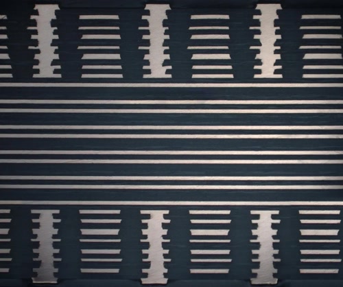
AI Accelerator Card Cross-section Image
Sunshine's high-speed technology expert team has developed a complete set of solutions for common problems and manufacturing challenges in AI accelerator card products. We can deeply cooperate with customers for AI accelerator card early-stage design simulation and later-stage PCB manufacturability production planning, meeting customers' high-density high-speed interconnection requirements.

