PCB copper-thickness unit—ounce (oz)
In PCB (printed circuit board) manufacturing, copper thickness refers to the thickness of the copper layer, usually measured in ounces (oz). Ounce (oz) itself is a unit of weight. The conversion formula between ounce and gram (g) is: 1 oz ≈ 28.35 g.

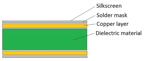
PCB Stack-up Copper Thickness
In the PCB industry, 1 oz means that copper weighing 1 oz is evenly spread over an area of 1 square foot (ft²). Expressed by formula, 1 oz = 28.35 g/ft².
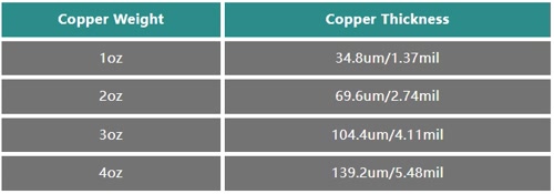
According to the mass calculation formula m = ρ (density) × V (volume) = ρ (density) × S (area) × t (thickness). That is, the weight of the copper foil divided by the density of copper and the area gives the copper foil thickness. Based on the calculation, the thickness of 1 oz copper is about 34.8 µm or 1.37 mil.

Copper Thickness Conversion Table
Copper thickness affects the current-carrying capacity of the circuit and the heat-dissipation performance of the PCB. Usually, the current-carrying capacity of a PCB trace can be increased by widening the line, but when routing space is limited, thicker copper must be used to meet the current-carrying requirement.
What factors affect the current-carrying capacity of a PCB conductor?
In August 2009, the IPC organization released the latest standard “IPC-2152, Standard for Determining Current Carrying Capacity in Printed Circuit Board Design”, replacing the previous old standard.
Conductor temperature rise (the temperature increment above ambient) is the decisive factor affecting the current-carrying capacity of a PCB conductor. The new IPC-2152 standard publishes, in the form of a set of nearly 100 charts, the relationship between PCB temperature rise and conductor current, trace width, trace thickness, PCB material, adjacent traces, inter-layer distance, presence or absence of coating, environmental conditions, and many other factors.

Factors Affecting Conductor Temperature Rise(ΔT above ambient)
PCB conductor current
Under the same conditions, the greater the current, the higher the temperature rise, and the lower the current-carrying capacity.
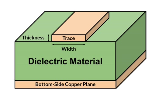
PCB conductor width
With the same cross-sectional area, the wider the trace, the better the heat dissipation, and the better the current-carrying capacity.
PCB conductor thickness
With the same cross-sectional area, the thinner the copper thickness of the conductor, the better the heat dissipation; the temperature rise of 1 oz is 5–10 % higher than that of 0.5 oz, the temperature rise of 2 oz is 10–15 % higher than that of 1 oz, and the temperature rise of 3 oz is 15–20 % higher than that of 2 oz.
PCB board thickness
Board thickness affects the path of heat transfer; the thicker the board, the better the heat dissipation. For the same FR-4 material, the conductor temperature rise of a 0.965 mm thick board is 30–40 % higher than that of a 1.79 mm thick board.
PCB material
The thermal conductivity of the material directly affects the temperature rise of the conductor; the greater the thermal conductivity, the lower the temperature rise. The thermal conductivity of copper is about 1,000 times that of FR-4, and the thermal conductivity of FR-4 is 10 times that of still air. Therefore, under still-air conditions, the temperature rise of internal conductors in a PCB will be smaller than that of external conductors.
Adjacent conductors on the same layer
If there are other conductors near the same layer of the trace, the heat-dissipation effect will be reduced; the more adjacent conductors on the same layer, the worse the heat dissipation, the higher the temperature rise, and the lower the current-carrying capacity.
Copper planes on adjacent layers
Copper planes on adjacent layers have the greatest influence on conductor temperature rise. Whether power planes, ground planes, or other copper planes, all help dissipate heat and thus reduce temperature rise. The closer the distance from the conductor to the adjacent copper plane, the lower the conductor temperature rise; the larger the area of the adjacent copper plane, the lower the conductor temperature rise; the thicker the adjacent copper plane, the lower the conductor temperature rise; the more adjacent copper planes there are, the lower the conductor temperature rise.
Surface coating
The solder-mask coating on the PCB surface also affects the heat-dissipation effect of the conductor; the thicker the coating, the worse the heat-dissipation effect, and the higher the temperature rise.
Estimating PCB trace width and copper thickness
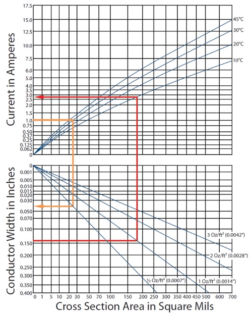
The following is the Conservative Chart given by IPC-2152. The important feature of the conservative chart is that it can cope with all situations, including internal and external conductors, PCB materials, PCB thickness, and environmental conditions such as air (except vacuum). The values obtained from this chart are very safe and valid under any condition (except vacuum), regardless of other variables.
When engineers design with reference to the conservative chart, although it is not optimal in terms of cost, area, etc., it will certainly meet the current and temperature-rise requirements.

IPC-2152 PCB power-trace width vs. current and temperature-rise chart
Source: Daniel Grillo
PCB trace width and the corresponding copper thickness can be calculated by looking up the IPC-2152 Conservative Chart.
As shown by the red arrow: PCB trace width 140 mil, using 1 oz copper thickness, vertically find the required temperature rise of 10 °C, then return to the y-axis to find the maximum current that can be passed: 2.75 A.
As shown by the orange arrow: if the PCB conductor needs to pass 1 A current and the target temperature rise is 30 °C, vertically downward find the required trace width under different copper thicknesses. For example, when using 0.5 oz copper thickness, the trace width needs to reach 40 mil.

