Copper foil is an important raw-material component of PCBs. The main functions of copper foil are to transmit current and signals; in addition, it can act as a reference plane to control the impedance of transmission lines or as a shielding layer to suppress electromagnetic interference.

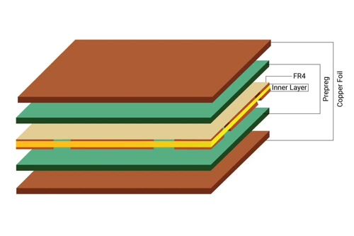
Copper Foil on FR4 Copper-clad Laminate
During PCB manufacture, properties such as copper-foil purity, thickness, surface roughness, peel strength, etching performance, and coefficient of thermal expansion also influence PCB quality and reliability.
Purity: Copper-foil purity is usually ≥ 99.5 %. High purity helps raise conductivity and reduces electrical problems caused by impurities.
Thickness (Weight): Copper-foil thickness is normally measured in ounces (oz). One-ounce copper foil can cover 1 square foot (ft²) and is about 1.4 mils (thousandths of an inch) thick. Copper thickness affects the current-carrying capacity of traces and the heat-dissipation performance of the PCB.
Peel Strength: The adhesion strength between copper foil and insulating substrate, expressed in newtons per metre (N/m), affects PCB mechanical stability and reliability.
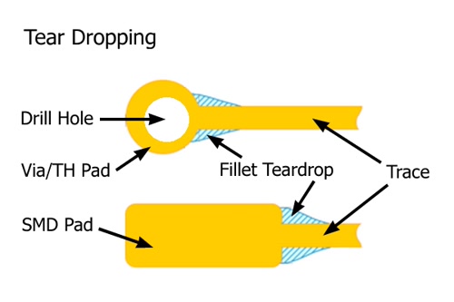
During PCB fabrication steps such as lamination, drilling, and plating, sufficient peel strength between copper foil and substrate is required to withstand thermal and mechanical stresses. If peel strength is insufficient, the foil may separate from the substrate during processing. As line widths shrink, copper-foil peel strength also drops; therefore, if conditions allow, teardrops can be added at pads to prevent trace lifting during soldering.

Add Teardrops At Pads
Coefficient of Thermal Expansion (CTE): The dimensional change per unit length of copper foil with temperature, influencing PCB dimensional stability and mechanical stress under differing temperatures. Copper-foil CTE should match that of other PCB materials to reduce thermal stress and improve reliability.
To improve PCB reliability, copper foil whose CTE matches that of other materials must be chosen, or lamination processes must be designed to lessen CTE mismatch among different materials. At the same time, temperatures during PCB fabrication must be accurately controlled to reduce quality problems caused by thermal expansion.
Etchability: During PCB manufacture copper foil must undergo an etching step to form the required circuit pattern; etchability affects etching quality and efficiency. Etching quality covers: precision of the etching process, etching uniformity, and surface smoothness after etching.
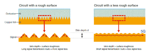
Surface Roughness: Copper-foil surface roughness affects its bond strength to insulating materials and solderability; for high-speed signals, however, the smoother the copper surface the better.

SEM Photos of Copper Surfaces with Differing Roughness
When signal frequency rises, current in PCB traces concentrates and flows within a certain depth at the surface, an effect called skin effect. The smoother the copper-foil surface, the less signal attenuation during propagation and the better the impedance control of the corresponding transmission line.

Influence of Copper-Surface Roughness on Signal Transmission
Brief Introduction to Copper-Foil Types
By manufacturing process, copper foil falls into two categories: Rolled and Electrodeposited; copper foils produced by different processes each have their specific application scenarios.
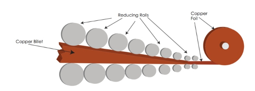
Rolled Annealed (RA): Produced by rolling an ingot into very thin foil; grain structure is horizontally oriented. Because rolling introduces stress in the foil, thermal annealing is needed to remove it. Both sides of rolled-annealed copper have comparatively high smoothness, so copper teeth must be created on the resin side during copper-clad-laminate processing to raise peel strength. Resin-side copper-tooth depth is generally about half that of electrodeposited copper teeth, so peel strength is also about half that of electrodeposited copper.
Because of its good surface smoothness, rolled-annealed copper foil shows excellent performance when transmitting signals above 13 GHz.

Rolled-Annealed Copper Foil
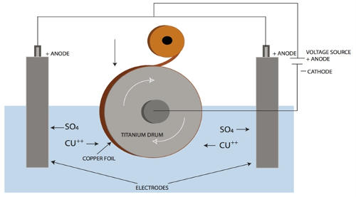
Electro Deposited (ED): Copper foil with vertically oriented grain structure produced by plating on a rotating drum. On the outer drum side the copper deposit is rough, providing strong peel strength, but it also causes comparatively large signal attenuation when transmitting high-frequency signals.

Electrodeposited Copper Foil
On the basis of the two basic manufacturing processes described above, many copper-foil types have been derived for differing application requirements.
High-Temperature Elongation (HTE): Also called HD copper foil, foil that retains excellent elongation at high temperature (180 °C). For 35 µm and 70 µm thick foils, elongation at high temperature (180 °C) can reach 4 %–10 %.
Reverse-Treated Foil (RTF): Also called reverse copper foil. On the basis of standard electrolytic copper foil (ED) or rolled-annealed copper foil (RA), the foil surface is roughened to improve its bonding performance with insulating materials (usually prepreg or pre-impregnated material).
The reverse-treated surface of RTF copper foil provides better adhesion, lowers the risk of interlayer peeling, and helps raise overall PCB structural stability.
Double-Side Treated (DST): Both shiny side and rough side are roughened, chiefly to lower cost; roughening the shiny side can eliminate copper-surface treatment and browning steps before film pressing. It can serve as inner-layer copper foil in multilayer boards, removing the need for browning treatment before multilayer lamination.
The drawback is that the copper surface may be scratched and, once contaminated, is difficult to clean.
Low-Profile (LP): “Low profile” is used here as a general term; still-lower-profile foils include VLP, HVLP, HVLP2, etc. Low-profile copper foil has very fine crystals (below 2 µm), equiaxed grains, no columnar crystals, and appears as flaky crystals with flat ridge lines, favouring signal transmission. At present LP copper foil is mainly used in high-frequency and high-speed PCBs.
Resin-Coated Copper (RCC): Also called resin-attached copper foil or adhesive copper foil. It is made by coating one or two layers of specially formulated resin solution (main component usually epoxy resin) on the roughened surface of thin electrolytic copper foil (thickness generally ≤ 18 µm), then drying in an oven to remove solvent so that the resin reaches a semi-cured stage.
RCC thickness used generally does not exceed 18 µm, 12 µm being common at present; resin-layer thickness is generally 40–100 µm. In build-up multilayer-board fabrication it replaces the traditional combination of prepreg and copper foil.
Ultra-Thin Foil (UTF): Refers to copper foil whose thickness is below 12 µm, commonly copper foil below 9 µm, used in fabricating PCBs with fine lines. Because extremely thin copper foil is difficult to handle, a carrier is generally used for support; carrier types include copper foil, aluminium foil, organic films, etc.
Statement: article content is compiled from open online material; copyright belongs to the original author and platform, used only for information sharing; contact us for deletion if infringement occurs.

