
Conventional Plated‑Through‑Hole (PTH) vias in multi‑layer PCBs run through the entire board. However, most high‑speed signals only require connections across a subset of layers. The unused, suspended copper segment left on the via is defined as a Via Stub.
Essentially, a via stub acts as an unterminated microstrip short stub, forming a λ/4 resonant cavity together with the main signal path. It reflects signal energy just like an “echo wall”. Longer stubs correspond to lower resonant frequencies.
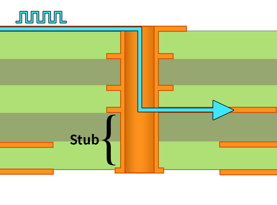
Via Stub
Based on the quarter‑wavelength resonance formula for via stubs: f = c/(4\times L\times\sqrt{Dk}) where:
c = speed of light
Full reflection occurs when the signal frequency $f$ satisfies the formula, meaning the stub equals one‑quarter of the effective wavelength. Parallel resonance takes place upon superposition of reflected and incident signals. This causes sharp impedance drop, massive signal energy reflection, degraded return loss, and pronounced insertion‑loss dips.
Take FR‑4 substrate ($Dk=4.0 @10\mathrm{GHz}$) as an example:
Practical measurements show an 8‑mil PTH stub can trigger a resonance dip worse than ‑15 dB at 12.5 GHz.
During PCB design, calculate the resonance frequency induced by stubs using the formula above. If the resonant frequency falls within the operating frequency band of your signal, stub mitigation measures are mandatory. For low‑speed thin PCBs, stubs impose negligible impact, so extra mitigation cost can be avoided.
Backdrilling, also known as Controlled‑Depth Drilling (CDD), uses a drill bit larger than the original PTH hole. It drills backward from the rear side of the board to remove excess plated‑copper via stubs for improved signal integrity.
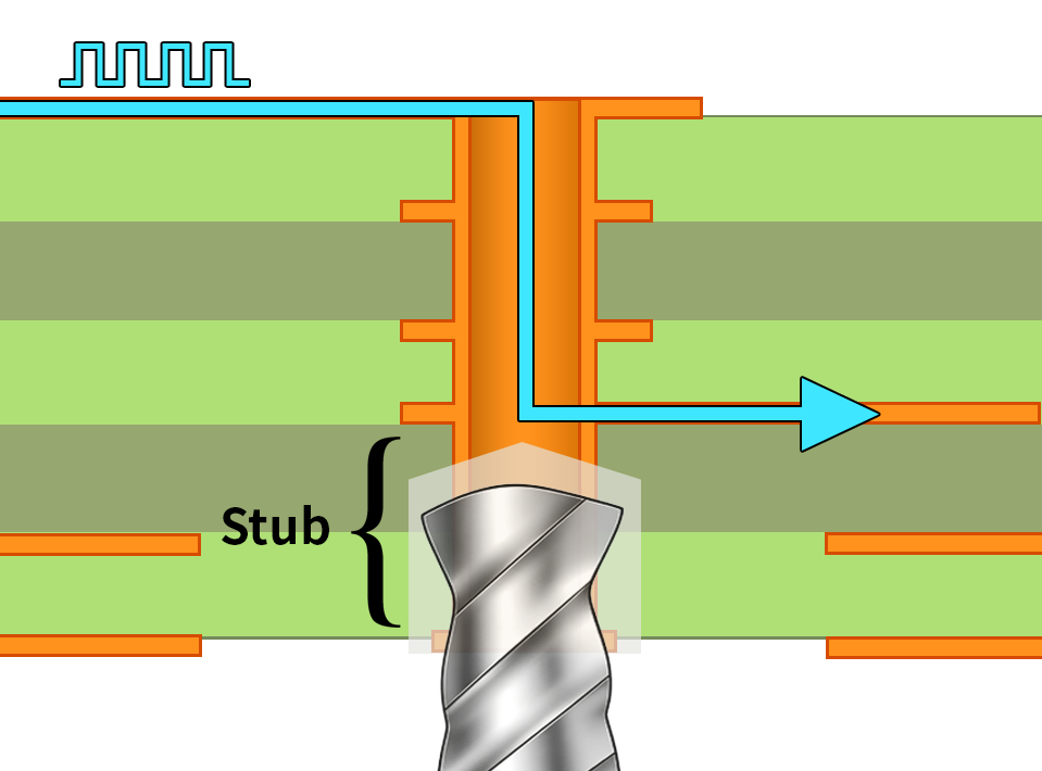
Backdrilling
Process sequence for backdrilling:
Complete standard PTH drilling, hole metallization and electroplating to form full‑thickness plated through‑holes.
For target stub length ≤10 mil: deploy a CDD machine with over‑sized drill bits. Drill from the stub‑side (back side of PCB) with precise depth control to remove stubs, while strictly maintaining tolerances so functional signal‑layer traces remain undamaged.
For target stub length ≤8 mil: 3D Back‑drilling plus Advanced Mapping is required.
Typical workflow:
Observe design‑for‑manufacturing rules for backdrilling at the PCB design stage to avoid specifications beyond fabricator process capability.
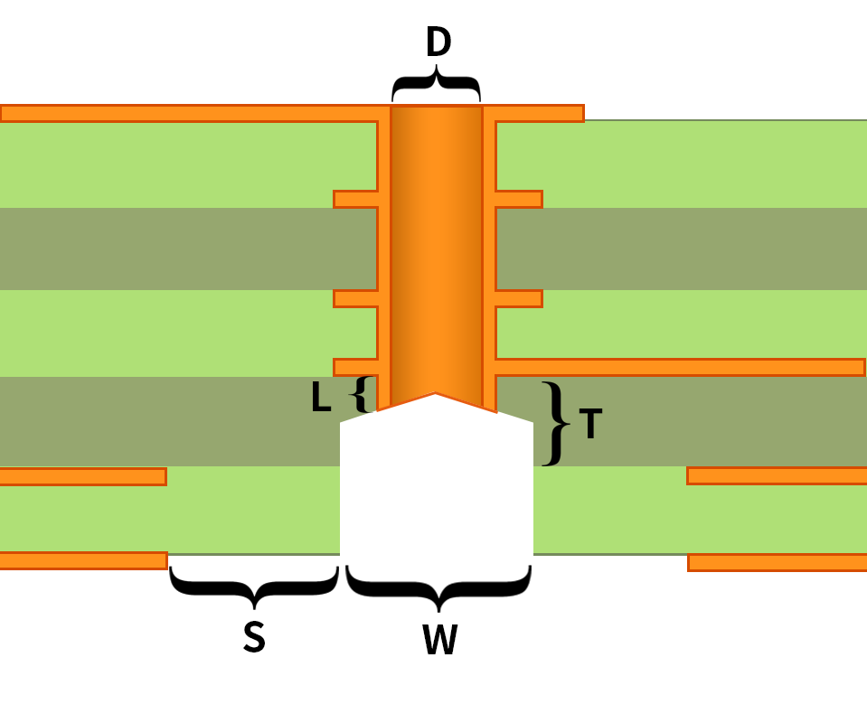
| Parameter | Description & Specification |
|---|---|
| D (Original via hole diameter) | 0.2‑0.5 mm. All finished vias shall be resin‑filled after backdrilling. |
| W (Back‑drilled hole diameter) | Determined by original via size. Normally 0.2 mm larger than the as‑drilled PTH hole; can be reduced to +0.15 mm in dense BGA regions. |
| S (Safety clearance) | ≥0.15 mm from back‑drill hole edge to pads / traces / copper pours. Minimum ≥0.125 mm allowed for dense BGA areas. |
| T (Dielectric thickness between drilled and non‑drilled layers) | ≥0.15 mm. Technical review is required for thickness below this threshold. |
| L (Stub residual length) | Conventional backdrilling: stub ≤10 mil. 3D backdrilling can achieve stub ≤6 mil. Higher via count and tighter stub tolerance will increase PCB fabrication cost. |
 WeChat