
As high‑power‑density power supplies, solid‑state transformers and other applications pursue miniaturization, light weight, high power density and high efficiency to the extreme, increasing the system operating frequency has become a core technical approach.
Raising the operating frequency can significantly reduce the volume and weight of magnetic components such as transformers and inductors, thereby driving power modules toward more compact configurations. Meanwhile, higher operating frequency facilitates soft‑switching technologies (e.g., LLC resonant converters), which effectively cut switching losses and improve the system dynamic response.
As current frequency rises, skin effect and proximity effect cause a sharp increase in conductor losses.
Skin Effect: High‑frequency current tends to flow along the conductor surface, leaving nearly no current in the conductor core. This reduces the effective conductive cross‑sectional area and makes the equivalent AC resistance far higher than the DC resistance.
Proximity Effect: Alternating currents in adjacent conductors generate alternating magnetic fields, which induce eddy currents inside neighboring conductors and further raise losses. Especially in multi‑layer windings or tightly‑coiled coils, the proximity effect can exert more severe impact than the skin effect.
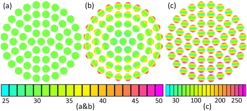
Figure: Current‑density distribution within strands of an ideal copper litz wire carrying 14 Apk current. Unit of the current‑density color bar: Apk/mm². (a) DC, self‑field condition; (b) 1 kHz, self‑field condition; (c) 1 kHz with an applied external 0.3 T magnetic field.
As illustrated above:
(a) DC self‑field: Current distributes uniformly within each strand with no skin or proximity‑effect influences.
(b) 1 kHz self‑field: The conductor’s own magnetic field triggers skin effect, concentrating current toward the edges of each strand.
(c) 1 kHz plus 0.3 T external field: In addition to the self‑field, magnetic fields from adjacent conductors introduce strong proximity effects. Current distribution becomes further skewed, leading to highly non‑uniform current across individual strands.
Litz wire is designed to address such high‑frequency loss challenges through two coordinated techniques: stranding and transposition.
Stranding: A single solid thick conductor is replaced by multiple thin, mutually insulated strands. Critically, the diameter of each individual strand must be far smaller than the skin depth at the target operating frequency. For instance, at 1 MHz, the optimal strand diameter is approximately one‑tenth of the skin depth (around 6.6 μm), ensuring skin effect is negligible for each strand.
Transposition / Twisting: Fine strands are braided or twisted so that each strand continuously changes its spatial position. In this way, every strand experiences all positions within the magnetic field equally, balancing induced voltage and current across strands and substantially suppressing eddy‑current losses caused by proximity effect.
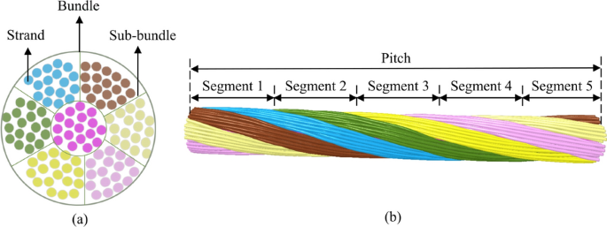
AC resistance modeling of Litz wire: integrating segmented equivalent circuit and twisting mechanism with VNS-based geometry model
Through stranding combined with transposition, litz wire distributes high‑frequency current evenly among all fine strands. Its AC resistance can be brought close to its DC resistance, fundamentally meeting the demand for low‑loss windings in high‑frequency, high‑current applications.
PCB litz wire mimics the winding architecture of conventional litz wire. PCB copper foils are split into multiple fine insulated “strands”. Special transposition patterns (e.g., vortex‑type structures) ensure each strand encounters identical magnetic‑flux conditions, balancing current distribution and mitigating skin‑effect and proximity‑effect‑driven AC losses at high frequencies.
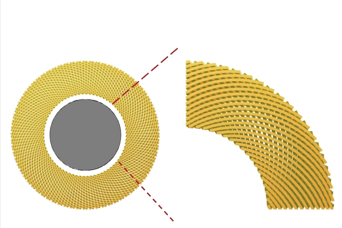
PCB litz wire
Structurally, PCB litz wire features a low‑profile form factor, making it suitable for space‑constrained applications.
In terms of thermal performance, FR‑4 exhibits higher thermal conductivity than air. Convection cooling performs better than traditional litz wire, which dissipates heat mostly via outer surfaces.
The excellent inter‑layer insulation property of PP materials used in PCBs suits high‑voltage scenarios requiring thick insulation (e.g., primary‑side windings for solid‑state transformers). It also eliminates reliability risks introduced by manual winding of conventional litz wire.
Benefiting from established PCB manufacturing workflows, PCB litz wire delivers high fabrication accuracy, consistent performance and controllable costs. It can be readily integrated with other circuit components such as drive and control circuits for high‑level modularization.
 WeChat