
Printed Circuit Board (PCB) manufacturers have commenced mass‑production of 112G‑grade PCBs, representing the highest‑data‑rate PCB product currently in volume production. Such boards impose special requirements in multiple aspects. First, 112G switch products adopt PAM4 (4‑level Pulse‑Amplitude Modulation), replacing the traditional NRZ (Non‑Return‑to‑Zero) coding scheme. PAM4 transmits four symbols (00, 01, 10, 11) within one symbol period, doubling the data throughput under the same bandwidth.
Nevertheless, the reduced voltage swing between signal levels weakens noise immunity and imposes stringent signal‑to‑noise ratio requirements. Even minor discontinuities along signal traces may trigger signal distortion, sharp Bit‑Error‑Rate (BER) degradation and decoding failure at the receiver end.
Impedance control therefore becomes critical for 112G hardware. Impedance tolerance has been tightened from ±10% to ±7%. Via impedance, previously unregulated, must now comply with the same tolerance as trace impedance. This new requirement prevents PCB fabricators from enlarging pin pads to ease registration challenges, since increasing the base pad size inevitably degrades via impedance.
Additionally, the Nyquist bandwidth of 112G signals reaches 28 GHz. The insertion loss of core‑material‑based PCBs is approximately 1 dB/inch (0.03937 dB/mm), meaning loss performance must be satisfied at 28 GHz. To shorten cycle time and reduce process steps, fabricators widely deploy deep micro‑via technology, where laser drills directly penetrate from Layer 1 down to Layer 3 or even Layer 4. This brings new challenges for PCB laser ablation and copper electroplating.
High‑speed signals travel from the optical‑module interface through an L1‑to‑L3 blind via to inner Layer 3. After a short differential trace on L3, signals pass through double‑sided back‑drilled vias to Layer 14. A long differential trace on L14 then routes signals via single‑sided back‑drilled vias toward the BGA (Ball‑Grid‑Array) footprint, completing the signal path.
Two comparative test groups were designed to characterize base‑pad influence on via impedance (see Table 1).

Simulation results are plotted in Figure 1. When the base pad is set to 0.4 mm, the via impedance reads 95 Ω, well‑matched against the target trace impedance of 93 Ω. With all other parameters unchanged, expanding the base pad to 0.55 mm pulls via impedance down to 85 Ω, substantially below the 93 Ω trace requirement. The resulting signal reflection drastically raises BER and leads to receiver decoding failure. Consequently, via‑impedance simulation shall be performed in the early‑stage design phase for 112G products to guarantee impedance consistency between vias and interconnect traces.
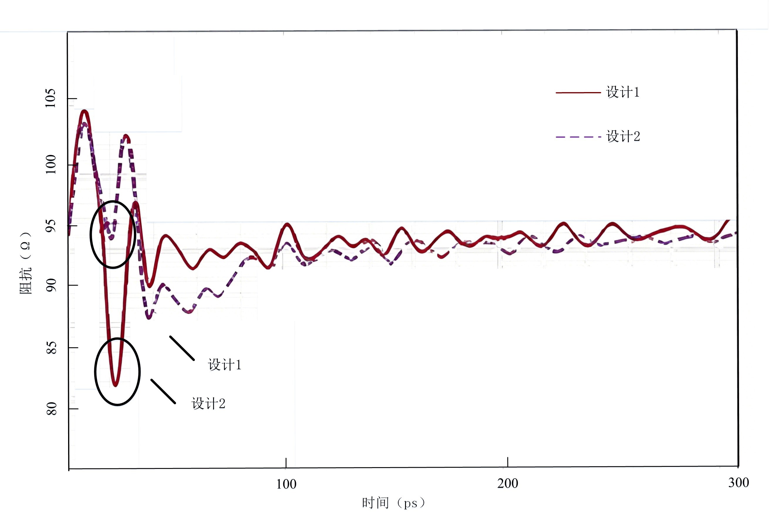
Figure 1: Simulated impedance curves with different base‑pad dimensions
To maintain impedance matching, base‑pad compensation cannot be over‑enlarged, which would tighten PCB manufacturing registration tolerances. Historically, our standard minimum annular‑ring width was 0.15 mm. Simulation shows that with a 0.25 mm hole diameter and 0.15 mm annular ring, the resultant 0.55 mm base‑pad yields only 85 Ω via impedance and fails specifications. The annular‑ring width must therefore be reduced to 0.075 mm, demanding blind‑via‑to‑pad registration better than 0.075 mm.
Two mainstream blind‑via alignment methodologies are available: registration against composite fiducial targets, or direct registration targeting the blind‑via base‑pad layer. Table 2 compares their pros and cons.
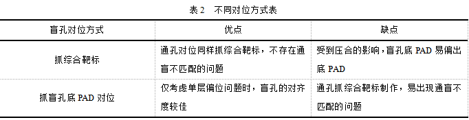
As illustrated in Figure 2, registering to blind‑via base‑pads achieves centered blind‑via alignment, yet risks layer‑to‑layer misalignment between through‑holes and blind vias. Outer‑layer exposure uses scaling factors derived from composite fiducials for through‑hole fabrication, whereas blind‑via exposure references single‑layer fiducials. Large deviation between composite and single‑layer scaling coefficients causes mis‑registration between outer‑layer through‑hole pads and blind vias.
A proprietary “plum‑blossom fiducial” pattern is implemented to resolve this issue. During blind‑via drilling, a ring of blind vias is drilled at each board corner. A through‑hole is subsequently drilled at the geometric center of each blind‑via ring to serve as the through‑hole fiducial (Figure 3). Outer‑layer exposure references both the surrounding blind‑via set and the central through‑hole fiducial at each corner. The outer‑layer scaling coefficient is thereby calculated as an averaged value for both via types, effectively mitigating blind‑via offset relative to outer‑layer pads.
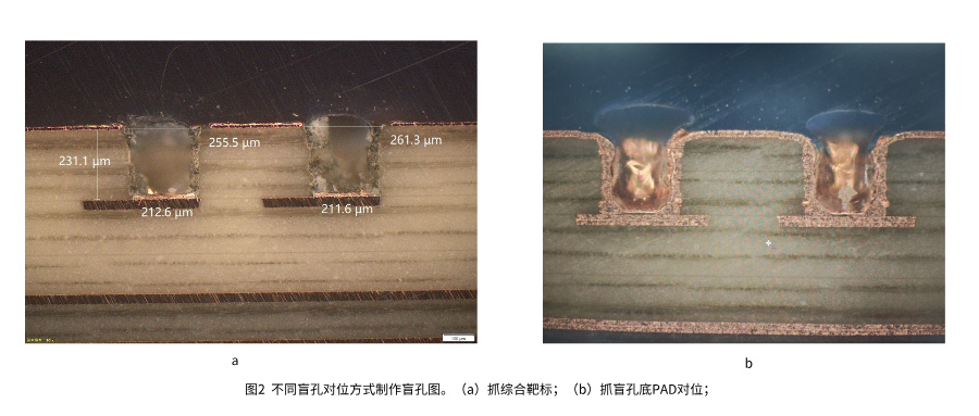
Figure 2: Cross‑section micrographs of blind vias under different alignment schemes (a) Composite‑fiducial registration; (b) base‑pad‑targeted blind‑via registration
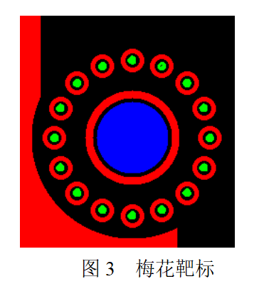
Figure 3: Schematic diagram of plum‑blossom fiducial pattern
To streamline manufacturing workflows, the original two‑press‑cycle process is replaced by a single‑press‑cycle flow. L1‑to‑L2 and L1‑to‑L3 blind vias are laser‑drilled after one lamination step. This imposes major challenges for both laser‑via formation and subsequent copper plating.
For L1‑to‑L3 blind‑via fabrication, isolation cut‑outs are implemented on intermediate Layer 2 directly above target blind‑via locations. Reaming operations are applied to control top‑to‑bottom aperture aspect ratios. Laser ablation adopts concentric spiral‑pattern drilling: peripheral rings are burned first, followed by inner regions, with 85 % overlap between adjacent laser spots. The blind‑via layout and spiral‑burning pattern are shown in Figure 4.
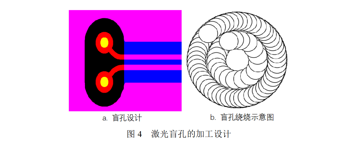
Figure 4: Laser blind‑via fabrication layout (a) Blind‑via layout sketch; (b) schematic of spiral laser‑burning sequence
For blind via fabrication to streamline the process flow and shorten manufacturing lead time, this product adopts a single lamination cycle instead of the original two‑lamination workflow. This means both L1‑to‑L2 and L1‑to‑L3 blind vias must be laser‑drilled in one batch. This approach introduces two major challenges: increased difficulty in blind via formation and greater complexity for subsequent copper plating.
In terms of blind via fabrication: To fabricate L1‑to‑L3 blind vias, isolation cutouts are first opened on Layer 2 directly above the target blind via locations. Next, reaming is applied to control the top‑to‑bottom aperture aspect ratio. The laser uses concentric spiral drilling for stacked microvias: the outer perimeter is ablated first, followed by the inner region. The laser spot overlap ratio is set at 85%. The blind via layout is shown in Figure 5.
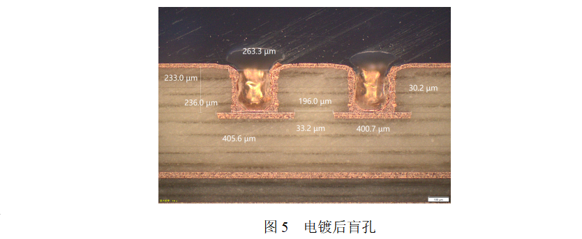
Figure 5: Cross‑section micrograph of electroplated blind vias
Back‑drill stub length must be strictly controlled for via‑impedance management. Excess stubs degrade via impedance and aggravate signal loss; limiting stub height constitutes a key signal‑integrity mitigation measure. According to customer pre‑simulation, a maximum allowable stub length of 0.2 mm satisfies transmission requirements, so our manufacturing spec enforces back‑drill stub length < 0.2 mm.
A batch‑partition and zone‑segmentation workflow is deployed to meet stub‑length requirements across the full board area:
Measure actual board thickness for all back‑drill locations. Split panels into separate batches where panel‑to‑panel thickness variation exceeds 0.1 mm; assign dedicated back‑drill parameters per batch.
Random cross‑section samples collected across different panel locations (Figure 6) confirm all stubs stay below the 0.2 mm specification.

Figure 6: Cross‑section micrographs of back‑drilled vias (a) Double‑sided back‑drill cross‑section; (b) single‑sided back‑drill cross‑section
This paper investigates via‑impedance challenges for 112 Gbps PCBs. Key design‑to‑fabrication control guidelines are summarized as below:
Conduct via‑impedance simulation during the design phase to achieve consistent impedance between vias and transmission traces.
Tighten blind‑via registration accuracy when reducing blind‑via base‑pad compensation for impedance optimization. For L1‑to‑L3 laser blind vias, copper‑plating thickness inside vias requires close monitoring.
 WeChat