
Thermal design is an essential aspect of reliability design. A well-designed thermal management system can prevent thermal failures on circuit boards and enhance their operational reliability. In the long term, it can also extend the service life of the circuit boards.
Most component specifications clearly state the operating junction temperature (TJ) of the components, with the highest operating temperature TJ-MAX often specified as 150°C. The goal of thermal design is to ensure that the highest junction temperature of the components during operation does not exceed the safe value.
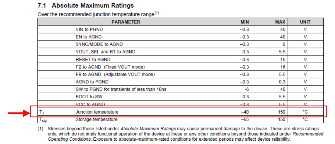
Range of Component Operating Temperature TJ
In actual engineering projects, many factors can affect the operating junction temperature (TJ) of components. As shown in the cross-sectional diagram of a mounted board-mounted switching power supply, factors such as component packaging, copper thickness of the outer and inner layers of the PCB, vias under components, and the area of thermal copper can all ultimately affect the highest junction temperature of components during operation.
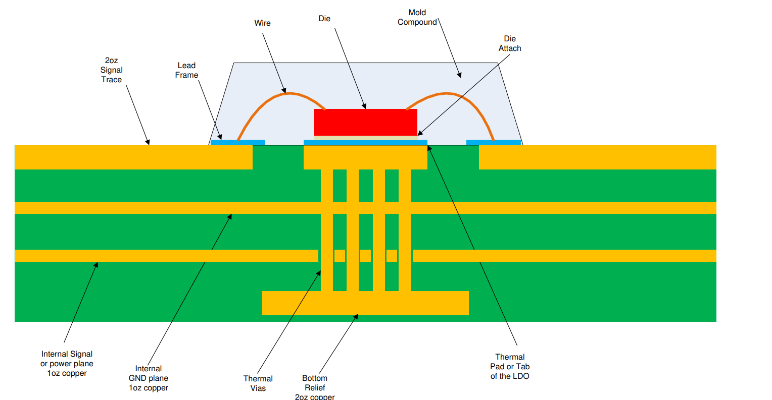
Cross-Sectional Diagram of a Board-Mounted Switching Power Supply
The operating junction temperature (TJ) of components can usually be calculated.

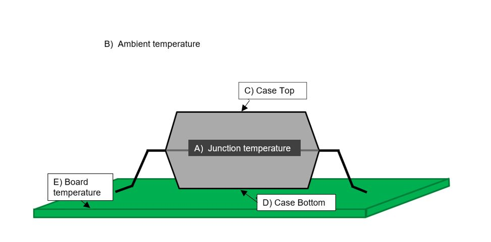
Key Indicators of Thermal Design
Generally, only by reducing dissipated power and thermal resistance can the requirements for junction temperature (TJ) be met. In actual design, high-efficiency switching power supply chips are used to reduce dissipated power, low thermal resistance chip packages are selected, and PCB materials are designed to increase the PCB heat dissipation area to reduce thermal resistance. Heat sinks and air or liquid cooling can also be used to reduce the operating temperature of components, but these cooling solutions are more expensive and can lead to an increase in product size.
Heat Dissipation Pie Chart
When cutting the heat dissipation plane, it is best to make radial cuts to avoid thermal bottlenecks in the heat dissipation path, allowing heat to radiate effectively. At the same time, it is necessary to ensure that the copper skin near the heat source is well connected to the heat source, so that the entire heat dissipation plane can play its role in heat dissipation.
Well-Split Heat Dissipation Plane in Layout
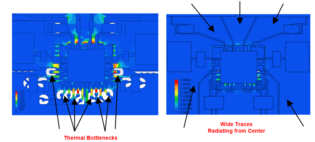
Heat Bottleneck in Poorly Radially Split Heat Dissipation Plane
For switching power supplies, DC/DC converters and inductors are key parts of energy loss. Typical design guidelines suggest placing inductors as close as possible to DC/DC converters to reduce EMI radiation. However, this can cause two heat sources to overlap, creating a local hot zone.
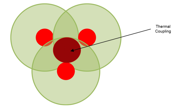
Hot Zone After Overlapping of Heat Sources
The "thermal footprint" of a heat-generating component is the area on the PCB that participates in the radiation and convection of the component's packaging, and its area is about 18 times the area of the component's packaging. If the thermal footprints overlap, the temperature of the components will rise sharply. The effect is most significant when the distance between packages is less than twice the size of the package.
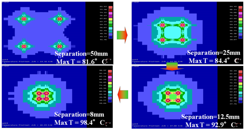
Thermal Footprints Produced by Different Heat Source Distances
In the engineering practice of board-mounted switching power supply layout, thermal design is only one of the many factors that need to be considered. Even many design guidelines conflict with the principles of thermal design. For example, to minimize the wiring area of switching devices, MOSFETs and inductors need to be as close as possible to the switching power supply chip. On the radial heat dissipation plane of the switching path, overly wide wiring can exacerbate EMI radiation. Therefore, in engineering practice, design needs to be considered comprehensively from multiple aspects. The following design practices can be referred to:
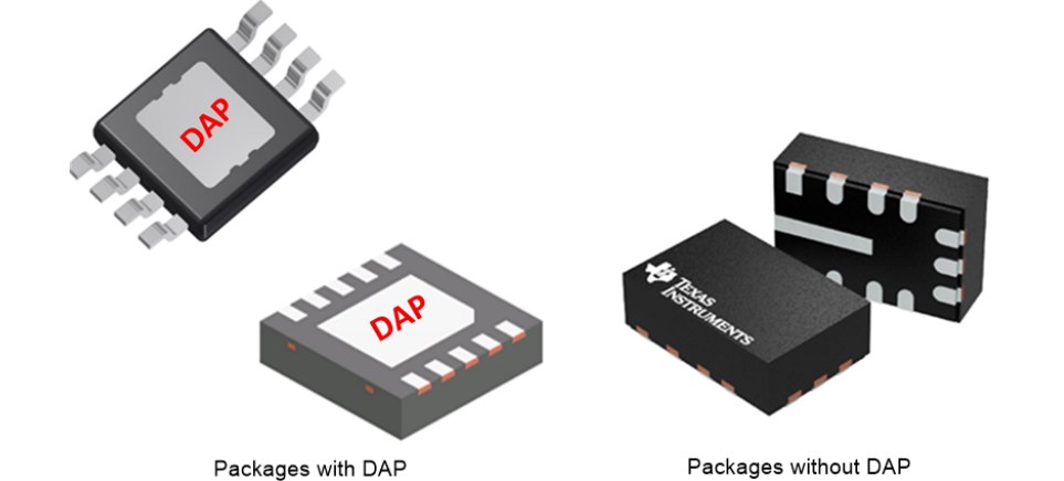
Choose components with low package thermal resistance, preferably using DAP packaged devices. The package is closest to the heat-generating core, and low package thermal resistance can significantly reduce the overall thermal resistance (θJA).
The heat dissipation copper surface on the same side as the heat source should be maximized. As the copper skin most closely connected to the heat source, it has the highest heat dissipation efficiency.
Use thick copper processes. Depending on the design requirements, thick copper processes of more than 3oz can be chosen. The thicker the copper, the lower the thermal resistance.
Widen the fan-out wire width of the heat source components as much as possible. The wider the wire width, the lower the thermal resistance.
Avoid breaking the continuous heat dissipation plane as much as possible, ensuring that there is a continuous heat dissipation plane in the radial heat dissipation direction of the heat source.
Use enough vias to connect the heat dissipation planes together, thereby reducing the thermal resistance of the entire heat dissipation plane and avoiding thermal bottlenecks.
Try to avoid crowding heat sources together. If space is limited and multiple heat sources are laid out close to each other, evaluate the use of heat sinks or air cooling.
Article reference source: PCB Thermal Design Tips for Automotive DC/DC Converters - Texas Instruments
Statement: The article content is organized from publicly available materials on the Internet, and the copyright belongs to the original author's platform. It is only used for information sharing. If there is any infringement, please contact to delete.