Why is PCIe 6.0 needed?
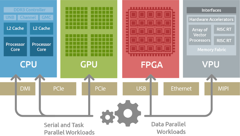
Since its official introduction in the early 21st century, the PCI Express (PCIe) interface has become the industry standard for chip-to-chip data transmission in data centers and computing applications. Specialized accelerator cards such as GPUs, FPGAs, and TPUs all use the PCIe interface to rapidly transfer data with various computing nodes.

Different chips' business flow data is transmitted through the PCIe interface.
Image source: ADLINK
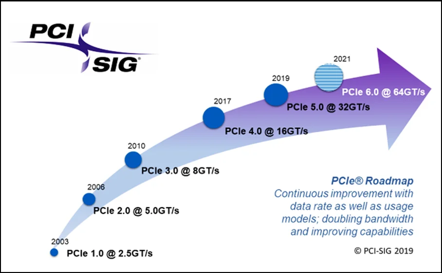
Since 2015, global data traffic has surged dramatically. As data centers transition to 100G Ethernet and beyond, PCIe interconnects in servers and network equipment have become a bottleneck. The chart below shows the evolution trend of PCIe standards. It can be seen that PCIe 2.0 to 3.0/4.0 took 5 and 7 years respectively. However, the time intervals from PCIe 4.0 to 5.0, and then to 6.0, were only 2 and 3 years respectively. Moreover, the 64GT/s transmission speed of PCIe 6.0 is 8 times that of the 3.0 standard.

The performance acceleration curve of PCIe
PCIe 6.0 Meets 800G Data Center Bandwidth Requirements
The PCIe 6.0 specification supports data centers' transition to 800G Ethernet. 800 Gb/s requires a bandwidth of 100 GB/s. In an x16 PCIe 6.0 link configuration, the unidirectional bandwidth can reach 128 GB/s. After link aggregation across multiple ports, it can fully support the bandwidth requirements of 1.6T Ethernet.
PCIe 6.0 Meets Multi-GPU Interconnect Requirements
NVLink focuses on data exchange between Nvidia GPUs, meeting the bandwidth requirements of high-performance computing tasks such as large-scale parallel processing and AI model training. PCIe, with its openness and broad compatibility, quickly adapts to market changes and technological evolution.
PCIe 6.0 provides a unidirectional transmission rate of up to 64 GT/s, significantly improving data throughput. In terms of energy efficiency, PCIe 6.0 adopts PAM-4 to optimize power consumption and signal integrity. Therefore, PCIe 6.0 has become the preferred choice for multi-GPU interconnects.
Memory Pool Sharing with Compute Express Link (CXL)
CXL 3.0 is based on the PCIe 6.0 protocol. CXL memory pool sharing technology supports unified memory addressing across CPU, GPU, FPGA and other devices. It can aggregate distributed memory into a shared pool and dynamically allocate it to different tasks. Through CXL-connected memory expansion cards, single server memory capacity can be increased from TB level to PB level, breaking through memory limitations for large model training while reducing the need for expensive HBM purchases.
NVMe
NVMe (Non-Volatile Memory Express) is a storage protocol specifically designed for solid-state drives (SSDs), aiming to fully utilize the high-speed bandwidth of the PCIe bus to provide high-performance, low-latency storage solutions. PCIe 6.0 provides higher bandwidth and lower latency for NVMe storage devices, significantly improving storage performance and energy efficiency, offering high-speed, low-latency storage solutions for data storage.
PCIe 6.0 Technical Features
Signal Channels and PAM-4 Modulation
PCIe 5.0 uses traditional NRZ (Non-Return-to-Zero) modulation. When the data rate reaches 32GT/s, the Nyquist frequency also reaches 16GHz. The increased frequency brings higher losses, coupled noise, and increased crosstalk, making the PCIe 5.0 channel the most difficult NRZ channel to handle.
PCIe 6.0 uses PAM-4 modulation. PAM-4 uses four signal levels (0, 1, 2, 3), forming three "eyes," with each level corresponding to two bits of data. This multi-level modulation significantly improves data transmission efficiency.
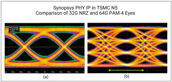
The eye diagram of PCIe 5.0 with a single eye compared to the three-eye diagram of PCIe 6.0
Both PCIe 5.0 and PCIe 6.0 have a signal Nyquist frequency of 16GHz. However, PAM-4's four voltage levels use 2-bit encoding in one UI, while NRZ uses 1-bit encoding, thus doubling the data rate.
Since the overall voltage swing at the transmitter (TX) doesn't increase, the available voltage for each eye in PAM-4 is only 1/3 of NRZ. Therefore, signals are more sensitive to noise, and the requirements for signal integrity between TX and RX are higher. Transitioning from NRZ to PAM-4 signals requires doubling the jitter requirements while causing a 9.6dB degradation in signal-to-noise ratio (SNR). Consequently, crosstalk and return loss in packaging and PCBs are also higher than in PCIe 5.0.
Forward Error Correction (FEC)
Increased noise sensitivity means the 1e-12 bit error rate (BER) we use for PCIe is not feasible, and Forward Error Correction (FEC) is needed because the BER of PAM-4 signaling will be several orders of magnitude higher than 1e-12. The target for the first bit error rate (FBER) is 1e-6. Forward Error Correction (FEC) compensates for this performance deficiency. The PCIe 6.0 specification limits additional FEC latency to 2 nanoseconds or less. To keep link retry rates low, FEC and CRC (Cyclic Redundancy Check) need to work together.
FLIT Mode
Therefore, PCIe 6.0 adopts 256-byte FLIT as the standard-sized data transmission unit. To support the fixed packet size requirements of FEC, PCIe 6.0 includes Flow Control Unit (FLIT)-based encoding. By eliminating the necessity of packet grouping at the physical layer, this modification also simplifies data management procedures, reduces latency, and improves efficiency.
Low Power Mode, FLIT Mode L0p
PCIe 6.0 introduces a new low-power state called L0p, allowing PCIe 6.0 links to scale bandwidth utilization without interrupting data flow, thereby reducing power consumption. In previous generations, changing link width would interrupt traffic for several microseconds during entire link retraining. However, L0p allows links to shut down channels, reducing power consumption while always maintaining at least one channel active, even when other channels are undergoing link training. It's important to note that this new low-power mode is only available in FLIT mode, while L0s supports non-FLIT mode.
This new low-power mode is symmetric, meaning TX and RX scale together, and retimers supporting FLIT mode also support this mode. During L0p, the PHY power consumption of idle channels is expected to be similar to when channels are turned off.
PCIe 6.0 PCB Material Selection
Since PCIe 6.0 uses PAM4 signaling, under 36 dB loss links, it's impossible to meet the 1E-06 bit error rate requirement. Therefore, the PCIe 6.0 specification has to reduce the total loss value of the entire physical channel to 32 dB.
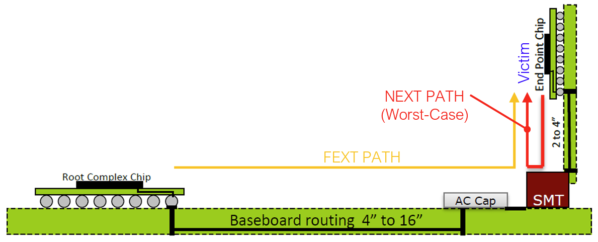
Schematic diagram of PCIe signal transmission link
As shown in the typical PCIe signal transmission link diagram above, PCIe cards establish signal transmission channels with chips on the motherboard through CEM connectors. Therefore, during signal transmission, losses occur from PCB trace losses, package losses, connector losses, via losses, etc. The PCIe 6.0 specification requirements for each part's losses are as follows:
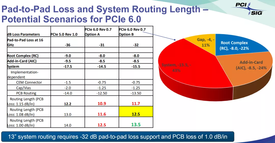
The PCIe 6.0 specification has stringent requirements for transmission loss to ensure reliable high-speed data transmission.
As shown in the PCIe 6.0 specification diagram above, the maximum loss generated by the PCB cannot exceed 13.5dB. Only when the PCB loss reaches 1.00dB/inch can the trace length reach the conventional 13.5inch length.
Currently, for PCIe 4.0 16GT/s speeds, motherboards already need to use Megtron 4/Megtron 6 materials. Considering that CPU chip sizes are continuously increasing, in the PCIe 5.0 and PCIe 6.0 era, motherboard PCB materials need to be further upgraded to Megtron 6/Megtron 7 grade. Copper foil types need to preferably use HVLP (Low Roughness) grade or above to reduce signal losses caused by skin effect.

