Advantages of PCB Bus Bar
The rapid development of new energy and energy storage industries drives the continuous improvement of power density in power supplies and batteries. After power density increases, requirements for power supply voltage fluctuation and heat dissipation also continue to improve.
Compared with traditional cables, PCB Bus Bar can provide more compact and efficient power distribution methods, while also reducing loop inductance, enhancing current carrying capacity, and improving overall system heat dissipation performance.

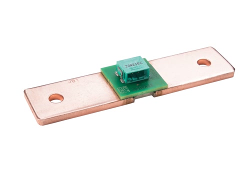
High Current PCB Bus Bar
PCB Bus Bar has the following advantages:
Reducing Power Loop Inductance
Through PCB Bus Bar, current can flow closely inside the equipment, reducing loop area, thereby reducing inductance values. In high-speed and high-frequency applications sensitive to power supply, PCB Bus Bar can reduce voltage spikes and noise, improving system stability.
Strong Current Carrying Capacity
Due to high-quality conductive materials and large cross-sectional area, PCB Bus Bar can efficiently carry large currents, particularly evident in high-current application scenarios such as power batteries and DC welding machines.
Improving Heat Dissipation Efficiency
PCB Bus Bar can effectively conduct heat generated by key heating components, thereby reducing additional heat dissipation requirements.
Space Saving
The compact design of PCB Bus Bar can also eliminate multiple wire connectors, saving space and reducing weight. Especially in aerospace and automotive industries that have requirements for equipment size and weight.

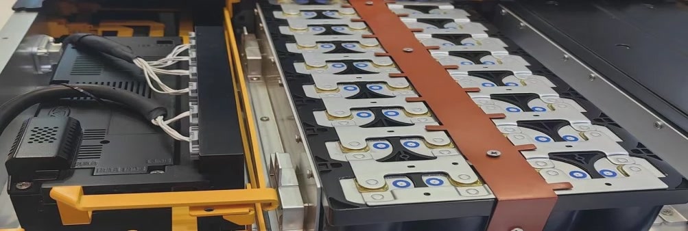
Power Battery PCB Bus Bar
Improving Reliability
Compared with traditional wiring systems, PCB Bus Bar has excellent mechanical strength and durability. Its robust structure can reduce connection loosening failures caused by vibration. Improves reliability in harsh environments and demanding applications.
Simplifying Assembly and Maintenance
Using PCB Bus Bar can reduce the number of cables and connectors used, simplifying the assembly process. This not only speeds up installation but also reduces assembly errors. Also facilitates later troubleshooting and maintenance.
PCB Bus Bar Design
When designing PCB Bus Bar, the following aspects should be considered:
Current Carrying Capacity and Heat Dissipation
PCB Bus Bar needs to effectively carry target current and not generate excessive heat under full load conditions.
Manufacturability and Cost
PCB Bus Bar design should not be overly complex. Current transmission paths need to be planned in advance to reduce the number and length of lines through PCB Bus Bar, lowering production difficulty.
Electromagnetic Compatibility
If high-frequency signals are coupled onto power or signals passing through PCB Bus Bar, then PCB Bus Bar may become an antenna, causing equipment to exceed external radiation limits. Therefore, electromagnetic compatibility requirements must be fully considered during circuit design.
The following points need attention during specific PCB Bus Bar design:
Copper Thickness
The thicker the copper, the greater the current carrying capacity, but thickness is not always better. Copper thickness needs to be calculated based on design voltage and current.
Current Capacity and Temperature Rise
The maximum carrying current of PCB Bus Bar design should be higher than full load requirements, while temperature rise must be kept within safe limits. These requirements are typically achieved by selecting appropriate conductor materials and optimizing conductor cross-sectional area. For example, for 100A current requirements, typical designs use copper strips with 5mm thickness, ensuring temperature rise does not exceed 20°C.

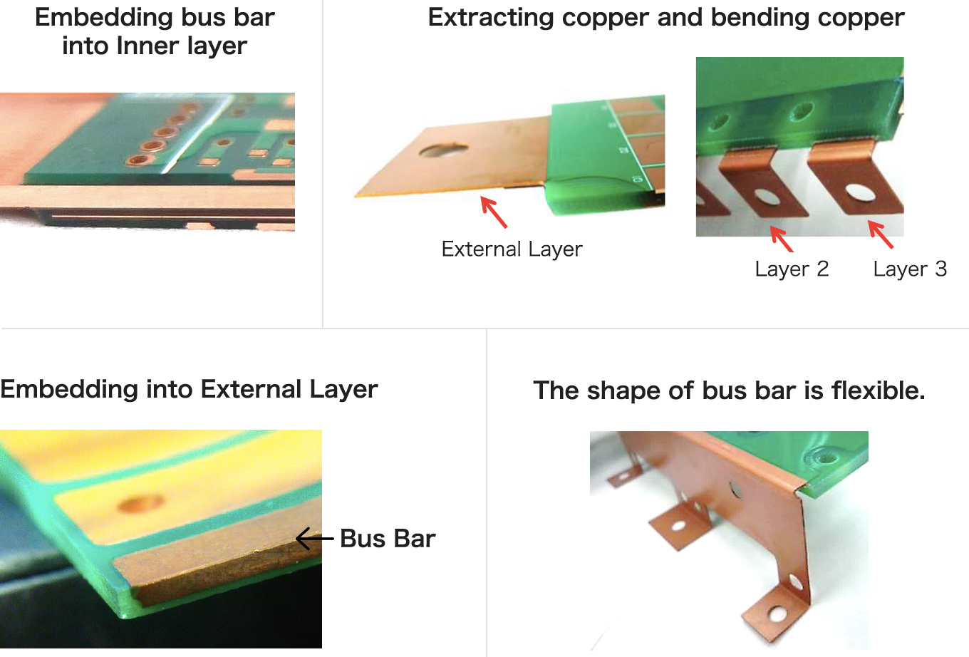
Multi-layer Flexible PCB Bus Bar Design
Bus Bar Resistance and Inductance
Low resistance and low inductance are key to PCB Bus Bar design. Conductor shape, thickness, and layout design all affect these parameters. For example, using trapezoidal or flat conductors can effectively reduce inductance, thereby improving current transmission efficiency.
Electromagnetic Compatibility (EMC)
PCB Bus Bar design needs to ensure it does not generate excessive electromagnetic interference (EMI) while resisting external electromagnetic interference. By optimizing conductor layout and using shielding materials to improve PCB Bus Bar electromagnetic compatibility.

