In PCB (Printed Circuit Board) manufacturing, copper thickness refers to the thickness of the copper layer, typically measured in ounces (oz). 1oz means the thickness achieved when 1oz of copper by weight is evenly distributed over an area of 1 square foot (ft²). The thickness of 1oz copper is approximately 35μm or 1.35mil.
Heavy copper PCB generally refers to PCBs with copper thickness exceeding 3 ounces (105μm). When wiring space is limited and increasing trace width cannot improve the current carrying capacity of PCB traces, using heavy copper PCB can effectively meet the current carrying requirements while improving PCB heat dissipation performance.

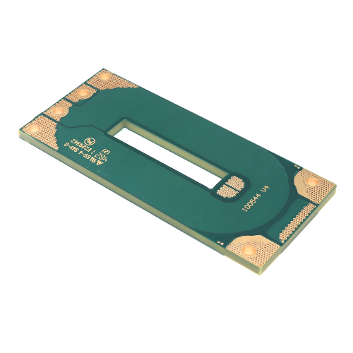
Planar Transformer (6oz copper thickness)
Advantages of Heavy Copper PCB:
High Current Carrying Capacity
Heavy copper PCB can carry sufficiently large current within limited space, effectively improving product power density.
Heat Conduction
Heavy copper layers can better conduct heat, thereby improving product heat dissipation performance while reducing PCB thermal expansion caused by temperature changes, improving PCB reliability.
Enhanced Mechanical Strength
Heavy copper layers can improve PCB mechanical strength, making it more stable and durable.
Heavy copper PCB is widely used in communication base station power supplies, server power supplies, welding equipment, energy storage systems, automotive power systems, aerospace, and other fields.
How to Estimate Required PCB Copper Thickness?
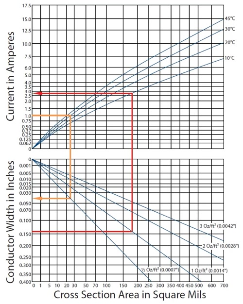
The following is the Conservative Chart provided by IPC-2152. The important aspect of the conservative chart is that it can handle all situations, including internal and external conductors, PCB materials, PCB thickness, and environmental conditions such as air (except vacuum). The values obtained from this chart are very safe and valid under any conditions (except vacuum environments), without considering other variables.
When engineers refer to the conservative chart for design, although it may not be optimal in terms of cost and area, it will definitely meet current and temperature rise requirements.

IPC 2152 PCB Power Trace Width vs Current and Temperature Rise Relationship Chart
Source: Daniel Grillo
You can calculate PCB trace width and select corresponding copper thickness by checking the IPC-2152 Conservative Chart.
As shown by the red arrow, for PCB trace width of 140 mil, using 1oz copper thickness, vertically find the corresponding temperature rise requirement of 10°C, then return to the y-axis to find the maximum current of 2.75A that can pass through.

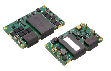
Power Brick (6oz copper thickness)
As shown by the orange arrow, if PCB conductor needs to pass 1A current with target temperature rise of 30°C, vertically downward find the required trace width for different copper thicknesses. When using 0.5oz copper thickness, trace width needs to reach 40mil.
Heavy Copper PCB Manufacturing Process
Due to thick copper thickness, heavy copper PCB brings a series of processing difficulties. Sunshine PCB has developed a heavy copper product line to systematically solve various manufacturing challenges of heavy copper PCB.
Heavy Copper PCB Etching
During the etching process, chemical exchange becomes more difficult, and side etching increases. Multiple rapid etching processes and increased etching compensation coefficients are needed to solve the problem of increased side etching.
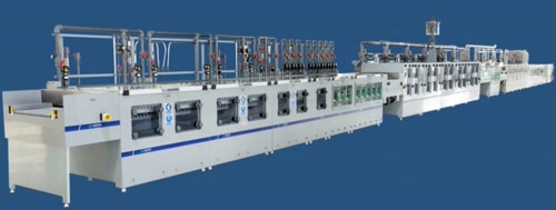
Sunshine PCB has customized a dedicated DES etching line for heavy copper, enabling one-time etching of 6oz heavy copper PCB.

Heavy Copper Dedicated DES Line
Heavy Copper PCB Lamination
During the lamination process, due to deep line gaps, when residual copper rate is the same, multiple sheets of prepreg with good flow properties need to be selected to meet resin filling requirements. At the same time, rivets need to be added to strengthen the fixation between core boards, reducing the risk of board slippage. Increased copper thickness causes the actual heating rate of boards during lamination to slow down, requiring extended duration of high-temperature segments to increase curing effect of prepreg.
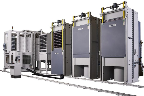
Sunshine PCB uses Burkle multi-layer lamination automatic production line and heavy copper dedicated browning solution to ensure lamination quality of heavy copper PCB. Currently, by combining Mass LAM and Pin LAM methods, we can produce up to 50-layer heavy copper PCB.

Burkle Lamination Press
Heavy Copper PCB Drilling
During the drilling process, when heavy copper board thickness exceeds 2.0mm, segmented drilling can be used to solve drilling difficulty problems. At the same time, adjust related parameters of feed speed and retract speed to optimize drilling quality, reduce cutting speed to avoid copper pad tearing problems.
Heavy Copper PCB Solder Mask
During solder mask printing, due to deep line gaps, height differences between copper and substrate can cause problems such as oil flow, insufficient oil thickness, line redness, pinhole bubbles, etc. Ink viscosity needs to be diluted and multiple printing processes used to solve these solder mask printing problems.
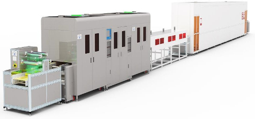
Sunshine PCB uses automatic solder mask spray line, adopting pre-treatment + double-sided spraying + pre-baking + fully automatic connection technology. By using special high-pressure nozzles + high-viscosity brand inks, we can complete 4OZ heavy copper one-time spraying. Solder mask thickness uniformity is good and soldering performance is friendly.

Automatic Solder Mask Spray Line

