
What is a planar transformer?
Module power supplies are widely used in the fields of communication and servo control. The miniaturization design of products has put forward more stringent requirements on transformers, such as small size, low profile, large output current, and small electromagnetic radiation. Traditional transformers have become an important factor restricting the further development of switching power supply technology.
At the same time, due to the eddy current effect, under high operating frequencies and large currents, the traditional wound magnetic components have problems such as a single coil structure, poor heat dissipation characteristics, and parameter inconsistency, which lead to significant increases in coil losses, not only reducing efficiency, but also causing increased temperature rise, increasing thermal design difficulties, and limiting further improvement in power density of switching power supplies. Therefore, there is an urgent need in the industry to study the coil loss model and develop new coil structures to reduce its losses, which is also a very important research content in high-frequency magnetic technology for power electronics.
Planar transformer is a new type of high-frequency ferrite inductance component that has been tried in the industry. Compared with traditional high-frequency transformers, planar transformers have the following characteristics:
High current density, able to meet the working characteristics of high-frequency current, with current density up to 30A/module;
High work efficiency, tight coupling between the primary and secondary sides, small leakage inductance, small cross-loss, but large distributed capacitance;
The utilization rate of the magnetic core window is low;
The transformer has fewer turns and larger magnetic flux, which is prone to saturation;
Better EMI, low leakage inductance means better EMI indicators for transformers, with minimal damage to switching power devices;
The shape is square and thin, suitable for surface mounting;
Good heat dissipation, high surface area ratio, short heat channel, and a structure that is conducive to heat dissipation;
High dielectric strength, with insulation design based on the required PCB layer and thickness;
The consistency is good.
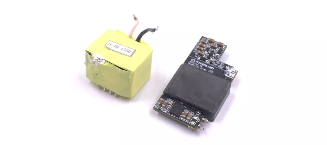
Ordinary transformers and planar transformers in gallium nitride charging heads
Structure Design of Planar Transformer
PCB winding structure
The winding of the planar transformer is achieved using a spiral trace on the PCB. The middle of the PCB is hollowed out for the installation of the magnetic core. The layers of the PCB are insulated by the board material. The magnetic core directly clamps the PCB in the middle and is then fixed with tape or clamps. The height of the planar transformer is effectively reduced, while further saving the volume. The PCB trace is flat, and the copper thickness is generally 1oz/2oz. By calculation, at frequencies less than 14MHz, the skin depth of copper is less than half of the thickness of the PCB copper. Usually, the frequency of the switching power supply is much lower than this value, so the skin effect of the planar transformer can be ignored.
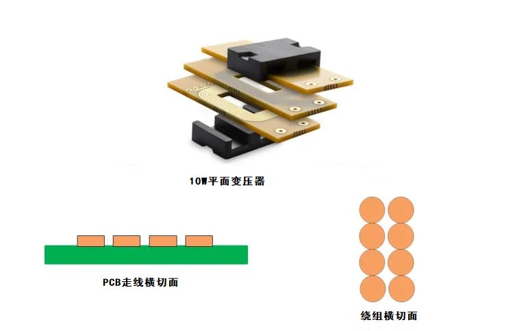
There are "through holes" between the layers of the PCB for winding interconnection, and the turns between the windings are connected in series or parallel through the "through holes".
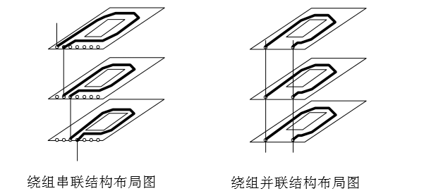
When the windings are connected in series, each printed board has a row of aligned through-holes, but only two of them are used for each layer of windings, thus achieving the series connection of windings. In low-voltage high-current applications, the overcurrent capability of the transformer can be improved by connecting the windings in parallel.
Magnetic core of planar transformer
Planar transformers generally use E-type, RM-type, EC, ETD, and EER magnetic cores made of high-frequency power ferrite soft magnetic materials.
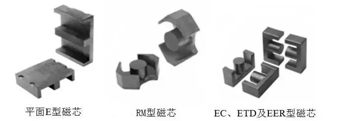
The E-type magnetic core has a simple manufacturing process and a relatively low price. It is currently the mainstream magnetic core shape for planar transformers. The E-type magnetic core has a large winding space, which provides enough space for large cross-sectional area winding and allows for high current flow. At the same time, the E-type magnetic core can be installed in different directions. Due to its excellent heat dissipation, it is commonly used in high-power transformers. Its disadvantage is that it cannot self-shield, and the middle column of the magnetic core is a rectangular parallelepiped, which cannot effectively utilize the space above the PCB to increase the length of the single-turn winding. At the same time, when the cross-sectional area of the PCB winding increases, the volume of the transformer is also relatively large.
The RM type of magnetic core has a circular shape both in the middle of the core and around the edges, which reduces the turn length of the copper wire and thus reduces copper loss. At the same time, it can make full use of the space above the PCB to reduce the cross-sectional area of the winding, designing the winding into a square shape, which results in less leakage inductance of the magnetic core. The shielding effect of the RM magnetic core is also better than that of the E type magnetic core.
EC, ETD, and EER type cores are between the E type and the RM type. This type of core, like the E type core, provides enough space for large cross-section leads to be drawn out, which is suitable for the trend of low-voltage high-current in switching power supplies. This type of core also has excellent heat dissipation due to the cylindrical shape of the middle column, which has some advantages over the E type. However, this type of core has the same poor shielding effect as the E type core.
PCB design of planar transformer
Design of multi-layer planar transformer
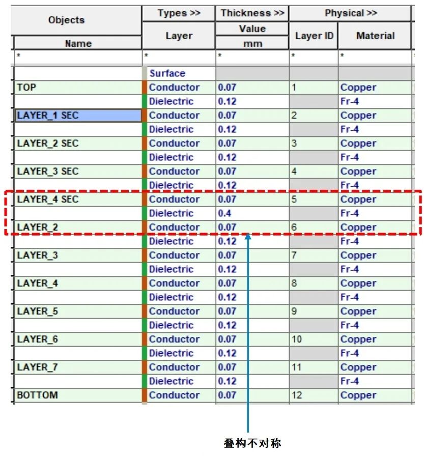
When designing a multilayer PCB for a planar transformer, it is recommended to use a symmetrical stacking design to avoid deformation during PCB processing and assembly. The thickness of the dielectric layers needs to meet the insulation requirements for the primary and secondary windings, and the dielectric thickness of the entire stack should be uniform.
Methods to reduce PCB manufacturing costs and delays
1: Select PP and Core with copper thickness and insulation that meet design requirements from the board materials recommended by the PCB manufacturer.
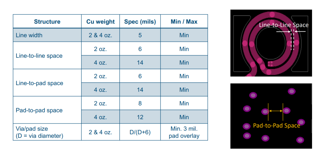
2: Thick copper can increase the impact of line width tolerance variations.
3: The thickness of the inner copper layer should not exceed 3oz.
4:If the thickness of the dielectric layer is greater than 0.2mm, the laser cannot penetrate the inner layer when making blind holes, requiring manual operation that increases costs and time.
5: Reduce the use of blind holes and buried holes.
6: The thickness tolerance of multilayer boards is relaxed to ±10%.
7:The design of the laminate determines the number of laminations, as shown in the following figure: The design materials of the laminate are unified, and the laminating can be completed in one step. As a comparison, the complex design of the laminate increases the number of laminations.
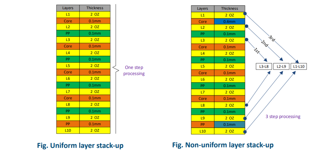
pressing times required for different laminating designs
8:Reduce the processing steps for drilling, align vias as much as possible, and preferably bury vias from L2-L3, L4-L5, L6-L7, L10-L11, avoiding going from one Core to another.
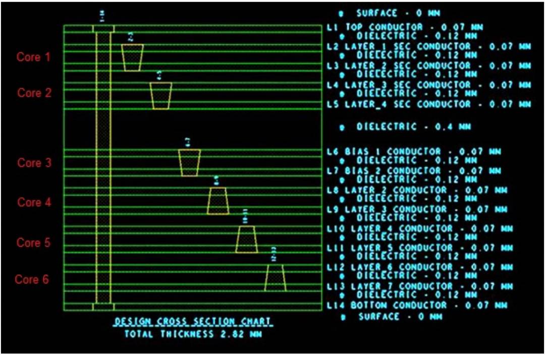
14-Layer Board Buried Hole and Through Hole Design
Note: The above content is collated from the Internet, and the copyright belongs to the original author. If there is any infringement, please contact us for deletion.